
2.6: Small Signal Model for Bipolar Transistor
- Page ID
- 88532

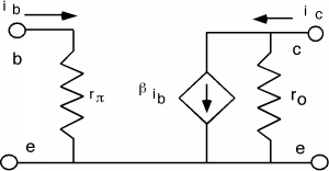
Thus, if we go back to the circuit model for the common emitter transistor and re-draw it as a small signal model, it would look something like Figure \(\PageIndex{1}\). Here we have replaced the diode with a linear element (a resistor, called \(r_{\pi}\)) and we have changed the notation for the currents from \(I_{B}\) and \(I_{C}\) to \(i_{b}\) and \(i_{c}\) respectively, to remind us that we are now talking about small signal ac quantities, not large signal ones. The bias currents \(I_{B}\) and \(I_{C}\) are still flowing through the device (and we will leave it to ELEC 342 to discuss how these are generated and set up) but they do not appear in the small signal model. This model is only used to figure out how the transistor behaves for the ac signal going through it, not how it responds to large DC values.
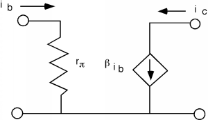
Now \(r_{\pi}\), the equivalent small signal resistance of the base-emitter diode, is given simply by the inverse of the conductance of the equivalent diode. Remember, we found \[\begin{array}{l} r_{\pi} &= \frac{1}{\frac{q}{kT} I_{B}} \\ &= \frac{1}{\frac{q}{kT} \frac{I_{C}}{\beta}} \\ &= \frac{\beta}{40 I_{C}} \end{array} \nonumber \]
where we have used the fact that \(I_{C} = \beta I_{B}\) and \(\frac{q}{kT} = 40 \mathrm{~V}^{-1}\). As we said earlier, typical values for \(\beta\) in a standard bipolar transistor will be around \(100\). Thus, for a typical collector bias current of \(I_{C} = 1 \mathrm{~mA}\), \(r_{\pi}\) will be about \(2.5 \mathrm{~k} \Omega\).
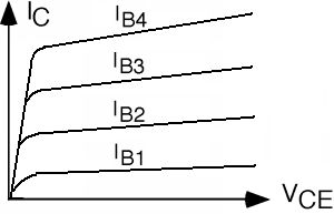
There is one more item we should consider in putting together our model for the bipolar transistor. We did not get things completely right when we drew the common emitter characteristic curves for the transistor. There is a somewhat subtle effect going on when \(V_{\text{CE}}\) is increased. Remember, we said that the current coming out of the collector is not effected by how big the drop was in the reverse biased base-collector junction. The collector current just depends on how many electrons are injected into the base by the emitter, and how many of them make it across the base to the base-collector junction. As the base-collector reverse bias is increased (by increasing \(V_{\text{CE}}\)) the depletion width of the base-collector junction increases as well. This has the effect of making the base region somewhat shorter. This means that a few more electrons are able to make it across the base region without recombining, and as a result \(\alpha\) and hence \(\beta\) increase somewhat. This then means that \(I_{C}\) goes up slightly with increasing \(V_{\text{CE}}\). The effect is called base width modulation. Let us now include that effect in the common emitter characteristic curves. As you can see in Figure \(\PageIndex{3}\), there is now a slope to the \(I_{C} \left(V_{\text{CE}}\right)\) curve, with \(I_{C}\) increasing somewhat as \(V_{\text{CE}}\) increases. The effect has been somewhat exaggerated in Figure \(\PageIndex{2}\), and I will now make the slope even bigger so that we may define a new quantity, called the Early Voltage.
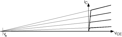
Back in the very beginning of the transistor era, an engineer at Bell Labs, Jim Early, predicted that there would be a slope to the \(I_{C}\) curves, and that they would all project back to the same intersection point on the horizontal axis. Having made that prediction, Jim went down into the lab, made the measurement, and confirmed his prediction, thus showing that the theory of transistor behavior was being properly understood. The point of intersection of the \(V_{\text{CE}}\) axis is known as the Early Voltage. Since the symbol \(V_{E}\), for the emitter voltage, was already taken, they had to label the Early Voltage \(V_{A}\) instead. (Even though the intersection point in on the negative half of the \(V_{\text{CE}}\) axis, \(V_{A}\) is universally quoted as a positive number.)
How can we model the sloping \(I \text{-} V\) curve? We can do almost the same thing as we did with the solar cell. The horizontal part of the curve is still a current source, and the sloped part is simply a resistor in parallel with it. Here is a graphical explanation in Figure \(\PageIndex{4}\).
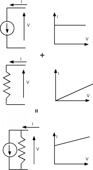
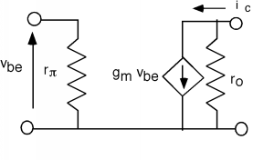
Usually, the slope is much less than we have shown here, and so for any given value of \(I_{C}\), we can just take the slope of the line as \(\frac{I_{C}}{V_{A}}\) and hence the resistance, which is usually called \(r_{o}\), is just \frac{V_{A}}{I_{C}}\). Thus, we add \(r_{o}\) to the small signal model for the bipolar transistor. This is shown in Figure \(\PageIndex{5}\). In a good quality modern transistor, the Early Voltage, \(V_{A}\) will be on the order of \(150 \text{-} 250 \mathrm{~V}\). So if we let \(V_{A} = 200 \mathrm{~V}\), and we imagine that we have our transistor biased at \(1 \mathrm{~mA}\), then \[\begin{array}{l} r_{o} &= \frac{200 \mathrm{~V}}{1 \mathrm{~mA}} \\ &= 200 \mathrm{~k} \Omega \end{array} \nonumber \]
which is usually much larger than most of the other resistors you will encounter in a typical circuit. In most instances, \(r_{o}\) can be ignored with no problem. If you get into high impedance circuits however, as you might find in a instrumentation amplifier, then \(v_{\text{be}}\) has to be taken into account.
Sometimes it is advantageous to use a mutual transconductance model instead of a current gain model for the transistor. If we call the input small signal voltage \(v_{\text{be}}\), then obviously \[\begin{array}{l} i_{b} &= \frac{v_{\text{be}}}{r_{\pi}} \\[4pt] &= \frac{v_{\text{be}}}{\frac{\beta}{40 I_C}} \end{array} \nonumber \]
But \[i_{c} = \beta i_{b} = \frac{\beta v_{\text{be}}}{\frac{\beta}{40 I_C}} = 40 I_{C} v_{\text{be}} \equiv g_{m} v_{\text{be}} \nonumber \]
where \(g_{m}\) is called the mutual transconductance of the transistor. Notice that \(\beta\) has completely cancelled out in the expression for \(g_{m}\) and that \(g_{m}\) depends only upon the bias current, \(I_{C}\), flowing through the collector and not on any of the physical properties of the transistor itself!
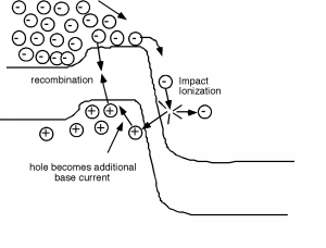
Finally, there is one last physical consideration we should make concerning the operation of the bipolar transistor. The base-collector junction is reverse biased. We know that if we apply too much reverse bias to a pn junction, it can breakdown through avalanche multiplication. Breakdown in a transistor is somewhat "softer" than for a simple diode, because once a small amount of avalanche multiplication starts, extra holes are generated within the base-collector junction. These holes fall up, into the base, where they act as additional base current, which, in turn, causes \(I_{C}\) to increase. This is shown in Figure \(\PageIndex{7}\).
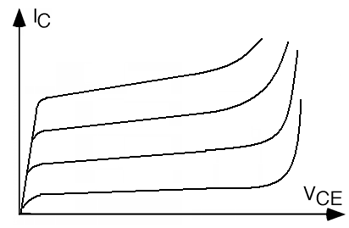
A set of characteristic curves for a transistor going into breakdown is also shown in Figure \(\PageIndex{8}\).
Well, we have learned quite a bit about bipolar transistors in a very short space. Go back over this chapter and see if you can pick out the two or three most important ideas of equations which would make up a set of "facts" that you could stick away in you head someplace. Do this so you will always have them to refer to when the subject of bipolars comes up (In, say, a job interview or something!).