
3.2: Basic MOS Structure
- Page ID
- 88534

\( \newcommand{\vecs}[1]{\overset { \scriptstyle \rightharpoonup} {\mathbf{#1}} } \)
\( \newcommand{\vecd}[1]{\overset{-\!-\!\rightharpoonup}{\vphantom{a}\smash {#1}}} \)
\( \newcommand{\dsum}{\displaystyle\sum\limits} \)
\( \newcommand{\dint}{\displaystyle\int\limits} \)
\( \newcommand{\dlim}{\displaystyle\lim\limits} \)
\( \newcommand{\id}{\mathrm{id}}\) \( \newcommand{\Span}{\mathrm{span}}\)
( \newcommand{\kernel}{\mathrm{null}\,}\) \( \newcommand{\range}{\mathrm{range}\,}\)
\( \newcommand{\RealPart}{\mathrm{Re}}\) \( \newcommand{\ImaginaryPart}{\mathrm{Im}}\)
\( \newcommand{\Argument}{\mathrm{Arg}}\) \( \newcommand{\norm}[1]{\| #1 \|}\)
\( \newcommand{\inner}[2]{\langle #1, #2 \rangle}\)
\( \newcommand{\Span}{\mathrm{span}}\)
\( \newcommand{\id}{\mathrm{id}}\)
\( \newcommand{\Span}{\mathrm{span}}\)
\( \newcommand{\kernel}{\mathrm{null}\,}\)
\( \newcommand{\range}{\mathrm{range}\,}\)
\( \newcommand{\RealPart}{\mathrm{Re}}\)
\( \newcommand{\ImaginaryPart}{\mathrm{Im}}\)
\( \newcommand{\Argument}{\mathrm{Arg}}\)
\( \newcommand{\norm}[1]{\| #1 \|}\)
\( \newcommand{\inner}[2]{\langle #1, #2 \rangle}\)
\( \newcommand{\Span}{\mathrm{span}}\) \( \newcommand{\AA}{\unicode[.8,0]{x212B}}\)
\( \newcommand{\vectorA}[1]{\vec{#1}} % arrow\)
\( \newcommand{\vectorAt}[1]{\vec{\text{#1}}} % arrow\)
\( \newcommand{\vectorB}[1]{\overset { \scriptstyle \rightharpoonup} {\mathbf{#1}} } \)
\( \newcommand{\vectorC}[1]{\textbf{#1}} \)
\( \newcommand{\vectorD}[1]{\overrightarrow{#1}} \)
\( \newcommand{\vectorDt}[1]{\overrightarrow{\text{#1}}} \)
\( \newcommand{\vectE}[1]{\overset{-\!-\!\rightharpoonup}{\vphantom{a}\smash{\mathbf {#1}}}} \)
\( \newcommand{\vecs}[1]{\overset { \scriptstyle \rightharpoonup} {\mathbf{#1}} } \)
\(\newcommand{\longvect}{\overrightarrow}\)
\( \newcommand{\vecd}[1]{\overset{-\!-\!\rightharpoonup}{\vphantom{a}\smash {#1}}} \)
\(\newcommand{\avec}{\mathbf a}\) \(\newcommand{\bvec}{\mathbf b}\) \(\newcommand{\cvec}{\mathbf c}\) \(\newcommand{\dvec}{\mathbf d}\) \(\newcommand{\dtil}{\widetilde{\mathbf d}}\) \(\newcommand{\evec}{\mathbf e}\) \(\newcommand{\fvec}{\mathbf f}\) \(\newcommand{\nvec}{\mathbf n}\) \(\newcommand{\pvec}{\mathbf p}\) \(\newcommand{\qvec}{\mathbf q}\) \(\newcommand{\svec}{\mathbf s}\) \(\newcommand{\tvec}{\mathbf t}\) \(\newcommand{\uvec}{\mathbf u}\) \(\newcommand{\vvec}{\mathbf v}\) \(\newcommand{\wvec}{\mathbf w}\) \(\newcommand{\xvec}{\mathbf x}\) \(\newcommand{\yvec}{\mathbf y}\) \(\newcommand{\zvec}{\mathbf z}\) \(\newcommand{\rvec}{\mathbf r}\) \(\newcommand{\mvec}{\mathbf m}\) \(\newcommand{\zerovec}{\mathbf 0}\) \(\newcommand{\onevec}{\mathbf 1}\) \(\newcommand{\real}{\mathbb R}\) \(\newcommand{\twovec}[2]{\left[\begin{array}{r}#1 \\ #2 \end{array}\right]}\) \(\newcommand{\ctwovec}[2]{\left[\begin{array}{c}#1 \\ #2 \end{array}\right]}\) \(\newcommand{\threevec}[3]{\left[\begin{array}{r}#1 \\ #2 \\ #3 \end{array}\right]}\) \(\newcommand{\cthreevec}[3]{\left[\begin{array}{c}#1 \\ #2 \\ #3 \end{array}\right]}\) \(\newcommand{\fourvec}[4]{\left[\begin{array}{r}#1 \\ #2 \\ #3 \\ #4 \end{array}\right]}\) \(\newcommand{\cfourvec}[4]{\left[\begin{array}{c}#1 \\ #2 \\ #3 \\ #4 \end{array}\right]}\) \(\newcommand{\fivevec}[5]{\left[\begin{array}{r}#1 \\ #2 \\ #3 \\ #4 \\ #5 \\ \end{array}\right]}\) \(\newcommand{\cfivevec}[5]{\left[\begin{array}{c}#1 \\ #2 \\ #3 \\ #4 \\ #5 \\ \end{array}\right]}\) \(\newcommand{\mattwo}[4]{\left[\begin{array}{rr}#1 \amp #2 \\ #3 \amp #4 \\ \end{array}\right]}\) \(\newcommand{\laspan}[1]{\text{Span}\{#1\}}\) \(\newcommand{\bcal}{\cal B}\) \(\newcommand{\ccal}{\cal C}\) \(\newcommand{\scal}{\cal S}\) \(\newcommand{\wcal}{\cal W}\) \(\newcommand{\ecal}{\cal E}\) \(\newcommand{\coords}[2]{\left\{#1\right\}_{#2}}\) \(\newcommand{\gray}[1]{\color{gray}{#1}}\) \(\newcommand{\lgray}[1]{\color{lightgray}{#1}}\) \(\newcommand{\rank}{\operatorname{rank}}\) \(\newcommand{\row}{\text{Row}}\) \(\newcommand{\col}{\text{Col}}\) \(\renewcommand{\row}{\text{Row}}\) \(\newcommand{\nul}{\text{Nul}}\) \(\newcommand{\var}{\text{Var}}\) \(\newcommand{\corr}{\text{corr}}\) \(\newcommand{\len}[1]{\left|#1\right|}\) \(\newcommand{\bbar}{\overline{\bvec}}\) \(\newcommand{\bhat}{\widehat{\bvec}}\) \(\newcommand{\bperp}{\bvec^\perp}\) \(\newcommand{\xhat}{\widehat{\xvec}}\) \(\newcommand{\vhat}{\widehat{\vvec}}\) \(\newcommand{\uhat}{\widehat{\uvec}}\) \(\newcommand{\what}{\widehat{\wvec}}\) \(\newcommand{\Sighat}{\widehat{\Sigma}}\) \(\newcommand{\lt}{<}\) \(\newcommand{\gt}{>}\) \(\newcommand{\amp}{&}\) \(\definecolor{fillinmathshade}{gray}{0.9}\)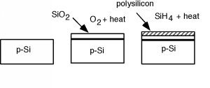
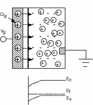
Figure \(\PageIndex{1}\) shows the steps necessary to make the MOS structure. It will help us in our understanding if we now rotate our picture so that it is pointing sideways in our next few drawings. (Also, we will forget about the two n-regions for awhile, and pick them back up later when we rotate the structure right side up again.) Figure \(\PageIndex{2}\) shows the rotated structure. Note that in the p-silicon we have positively charged mobile holes, and negatively charged, fixed acceptors. Because we will need it later, we have also shown the band diagram for the semiconductor below the sketch of the device. Note that since the substrate is p-type, the Fermi level is located down close to the valance band.
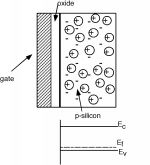
Figure \(\PageIndex{2}\): Basic MOS structure
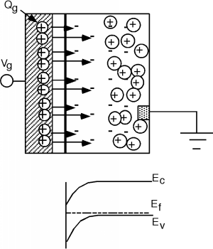
Let us now place a potential between the gate and the silicon substrate. Suppose we make the gate negative with respect to the substrate. Since the substrate is p-type, it has a lot of mobile, positively charged holes in it. Some of them will be attracted to the negative charge on the gate, and move over to the surface of the substrate. This is also reflected in the band diagram below the sketch of the structure in Figure \(\PageIndex{3}\). Remember that the density of holes is exponentially proportional to how close the Fermi level is to the valence band edge. We see that the band diagram has been bent up slightly near the surface to reflect the extra holes which have accumulated there.
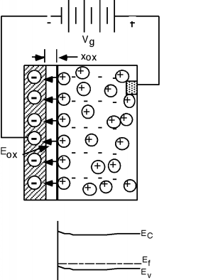
Figure \(\PageIndex{3}\): Applying a negative gate voltage
An electric field will develop between the positive holes and the negative gate charge. Note that the gate and the substrate form a kind of parallel plate capacitor, with the oxide acting as the insulating layer in between them. The oxide is quite thin compared to the area of the device, and so it is quite appropriate to assume that the electric field inside the oxide is a uniform one. (We will ignore fringing at the edges.) The integral of the electric field is just the applied gate voltage \(V_{g}\). If the oxide has a thickness \(x_{\text{ox}}\), then since \(E_{\text{ox}}\) is uniform, it is given by \[E_{\text{ox}} = \frac{V_{g}}{x_{\text{ox}}}\]
If we focus in on a small part of the gate, we can make a little "pill" box which extends from somewhere in the oxide, across the oxide/gate interface and ends up inside the gate material someplace. The pill box will have an area \(\Delta (s)\). Now we will invoke Gauss's law, which we reviewed earlier. Gauss's law simply says that the surface integral over a closed surface of the displacement vector \(D\) (which is, of course, just \(\varepsilon\) times \(E\)) is equal to the total charge enclosed by that surface. We will assume that there is a surface charge density \(-Q_{g}\), in units of \(\frac{\mathrm{Coulombs}}{\mathrm{cm}^2}\) on the surface of the gate electrode (Figure \(\PageIndex{4}\). The integral form of Gauss's Law is just: \[\oint \varepsilon_{\text{ox}} \mathbf{E} \ d \mathbf{S} = Q_{\text{encl}}\]
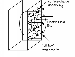
Figure \(\PageIndex{4}\): Finding the surface charge density
Note that we have used \(\varepsilon_{\text{ox}} E\) in place of \(D\). In this particular setup the integral is easy to perform, since the electric field is uniform, and only pointing in through one surface — it terminates on the negative surface charge inside the pill box. The charge enclosed in the pill box is just \(Q_{g} \Delta (s)\), and so we have (keeping in mind that the surface integral of a vector pointing into the surface is negative) \[\begin{array}{l} \oint \varepsilon_{\text{ox}} \mathbf{E} \ d \mathbf{S} &= -\left( \varepsilon_{\text{ox}} E_{\text{ox}} \Delta (s)\right) \\ &= - \left(Q_{g} \Delta (s)\right) \end{array}\]
or \[\varepsilon_{\text{ox}} E_{\text{ox}} = Q_{g}\]
Now, we can use Equation \(\PageIndex{1}\) to get \[\frac{\varepsilon_{\text{ox}} V_{g}}{x_{\text{ox}}} = Q_{g}\]
or \[\frac{Q_{g}}{V_{g}} = \frac{\varepsilon_{\text{ox}}}{x_{\text{ox}}} \equiv c_{\text{ox}}\]
The quantity \(c_{\text{ox}}\) is called the oxide capacitance. It has units of \(\frac{\mathrm{Farads}}{\mathrm{cm}^2}\), so it is really a capacitance per unit area of the oxide. The dielectric constant of silicon dioxide, \(\varepsilon_{\text{ox}}\), is about \(3.3 \times 10^{-13} \mathrm{~F} / \mathrm{cm}\). A typical oxide thickness might be \(250 \AA\), or \(2.5 \times 10^{-6} \mathrm{~cm}\). In this case, \(c_{\text{ox}}\) would be about \(1.30 \times 10^{-7} \ \frac{\mathrm{F}}{\mathrm{cm}^2}\). (The units we are using here, while they might seem a little arbitrary and confusing, are the ones most commonly used in the semiconductor business. You will get used to them in a short while.)
The most useful form of Equation \(\PageIndex{6}\) is when it is turned around: \[Q_{g} = c_{\text{ox}} V_{g}\]
as it gives us a way to find the charge on the gate in terms of the gate potential. We will use this equation later in our development of how the MOS transistor really works.
It turns out we have not done anything very useful by applying a negative voltage to the gate. We have drawn more holes there in what is called an accumulation layer, but that is not helping us in our effort to create a layer of electrons in the MOSFET which could electrically connect the two n-regions together.
Let's turn the battery around and apply a positive voltage to the gate. (Actually, let's take the battery out of the sketch for now, and just let \(V_{g}\) be a positive value, relative to the substrate which will tie to ground.) Making \(V_{g}\) positive puts positive \(Q_{g}\) on the gate. The positive charge pushes the holes away from the region under the gate and uncovers some of the negatively-charged fixed acceptors. Now the electric field points the other way and goes from the positive gate charge, terminating on the negative acceptor charge within the silicon.
The electric field now extends into the semiconductor. We know from our experience with the p-n junction that when there is an electric field, there is a shift in potential, which is represented in the band diagram by bending the bands. Bending the bands down (as we should moving towards positive charge) causes the valence band to pull away from the Fermi level near the surface of the semiconductor. If you remember the expression we had for the density of holes in terms of \(E_{v}\) and \(E_{f}\) (electron and hole density equations) it is easy to see that indeed \[p = N_{v} e^{- \frac{E_{f} - E_{v}}{kT}} \]
there is a depletion region (region with almost no holes) near the region under the gate. (Once \(E_{f} - E_{v}\) gets large with respect to \(kT\), the negative exponent causes \(p \rightarrow 0\).
The electric field extends further into the semiconductor, as more negative charge is uncovered and the bands bend further down. But now we have to recall the electron density equation, which tells us how many electrons we have: \[n = N_{c} e^{- \frac{E_{c} - E_{f}}{kT}}\]
A glance at Figure \(\PageIndex{6}\) above reveals that with this much band bending, \(E_{c}\), the conduction band edge, and \(E_{f}\), the Fermi level, are starting to get close to one another (at least compared to \(kT\)), which means that \(n\), the electron concentration, should soon start to become significant. In the situation represented by Figure \(\PageIndex{6}\), we say we are at threshold, and the gate voltage at this point is called the threshold voltage, \(V_{T}\).
Now, let's increase \(V_{g}\) above \(V_{T}\). Here's the sketch in Figure \(\PageIndex{7}\).
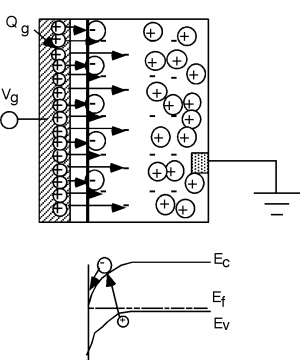
Even though we have increased \(V_{g}\) beyond the threshold voltage, \(V_{T}\), and more positive charge appears on the gate, the depletion region no longer moves back into the substrate. Instead electrons start to appear under the gate region, and the additional electric field lines terminate on these new electrons instead of on additional acceptors. We have created an inversion layer of electrons under the gate, and it is this layer of electrons which we can use to connect the two n-type regions in our initial device.
Where did these electrons come from? We do not have any donors in this material, so they can not come from there. The only place from which electrons could be found would be through thermal generation. Remember, in a semiconductor, there are always a few electron hole pairs being generated by thermal excitation at any given time. Electrons that get created in the depletion region are caught by the electric field and are swept over to the edge by the gate. I have tried to suggest this with the electron generation event shown in the band diagram in the figure. In a real MOS device, we have the two n-regions, and it is easy for electrons from one or both to "fall" into the potential well under the gate, and create the inversion layer of electrons.