
4.2: Measurement of Scattering Parameters
- Page ID
- 41107

\( \newcommand{\vecs}[1]{\overset { \scriptstyle \rightharpoonup} {\mathbf{#1}} } \)
\( \newcommand{\vecd}[1]{\overset{-\!-\!\rightharpoonup}{\vphantom{a}\smash {#1}}} \)
\( \newcommand{\id}{\mathrm{id}}\) \( \newcommand{\Span}{\mathrm{span}}\)
( \newcommand{\kernel}{\mathrm{null}\,}\) \( \newcommand{\range}{\mathrm{range}\,}\)
\( \newcommand{\RealPart}{\mathrm{Re}}\) \( \newcommand{\ImaginaryPart}{\mathrm{Im}}\)
\( \newcommand{\Argument}{\mathrm{Arg}}\) \( \newcommand{\norm}[1]{\| #1 \|}\)
\( \newcommand{\inner}[2]{\langle #1, #2 \rangle}\)
\( \newcommand{\Span}{\mathrm{span}}\)
\( \newcommand{\id}{\mathrm{id}}\)
\( \newcommand{\Span}{\mathrm{span}}\)
\( \newcommand{\kernel}{\mathrm{null}\,}\)
\( \newcommand{\range}{\mathrm{range}\,}\)
\( \newcommand{\RealPart}{\mathrm{Re}}\)
\( \newcommand{\ImaginaryPart}{\mathrm{Im}}\)
\( \newcommand{\Argument}{\mathrm{Arg}}\)
\( \newcommand{\norm}[1]{\| #1 \|}\)
\( \newcommand{\inner}[2]{\langle #1, #2 \rangle}\)
\( \newcommand{\Span}{\mathrm{span}}\) \( \newcommand{\AA}{\unicode[.8,0]{x212B}}\)
\( \newcommand{\vectorA}[1]{\vec{#1}} % arrow\)
\( \newcommand{\vectorAt}[1]{\vec{\text{#1}}} % arrow\)
\( \newcommand{\vectorB}[1]{\overset { \scriptstyle \rightharpoonup} {\mathbf{#1}} } \)
\( \newcommand{\vectorC}[1]{\textbf{#1}} \)
\( \newcommand{\vectorD}[1]{\overrightarrow{#1}} \)
\( \newcommand{\vectorDt}[1]{\overrightarrow{\text{#1}}} \)
\( \newcommand{\vectE}[1]{\overset{-\!-\!\rightharpoonup}{\vphantom{a}\smash{\mathbf {#1}}}} \)
\( \newcommand{\vecs}[1]{\overset { \scriptstyle \rightharpoonup} {\mathbf{#1}} } \)
\( \newcommand{\vecd}[1]{\overset{-\!-\!\rightharpoonup}{\vphantom{a}\smash {#1}}} \)
\(\newcommand{\avec}{\mathbf a}\) \(\newcommand{\bvec}{\mathbf b}\) \(\newcommand{\cvec}{\mathbf c}\) \(\newcommand{\dvec}{\mathbf d}\) \(\newcommand{\dtil}{\widetilde{\mathbf d}}\) \(\newcommand{\evec}{\mathbf e}\) \(\newcommand{\fvec}{\mathbf f}\) \(\newcommand{\nvec}{\mathbf n}\) \(\newcommand{\pvec}{\mathbf p}\) \(\newcommand{\qvec}{\mathbf q}\) \(\newcommand{\svec}{\mathbf s}\) \(\newcommand{\tvec}{\mathbf t}\) \(\newcommand{\uvec}{\mathbf u}\) \(\newcommand{\vvec}{\mathbf v}\) \(\newcommand{\wvec}{\mathbf w}\) \(\newcommand{\xvec}{\mathbf x}\) \(\newcommand{\yvec}{\mathbf y}\) \(\newcommand{\zvec}{\mathbf z}\) \(\newcommand{\rvec}{\mathbf r}\) \(\newcommand{\mvec}{\mathbf m}\) \(\newcommand{\zerovec}{\mathbf 0}\) \(\newcommand{\onevec}{\mathbf 1}\) \(\newcommand{\real}{\mathbb R}\) \(\newcommand{\twovec}[2]{\left[\begin{array}{r}#1 \\ #2 \end{array}\right]}\) \(\newcommand{\ctwovec}[2]{\left[\begin{array}{c}#1 \\ #2 \end{array}\right]}\) \(\newcommand{\threevec}[3]{\left[\begin{array}{r}#1 \\ #2 \\ #3 \end{array}\right]}\) \(\newcommand{\cthreevec}[3]{\left[\begin{array}{c}#1 \\ #2 \\ #3 \end{array}\right]}\) \(\newcommand{\fourvec}[4]{\left[\begin{array}{r}#1 \\ #2 \\ #3 \\ #4 \end{array}\right]}\) \(\newcommand{\cfourvec}[4]{\left[\begin{array}{c}#1 \\ #2 \\ #3 \\ #4 \end{array}\right]}\) \(\newcommand{\fivevec}[5]{\left[\begin{array}{r}#1 \\ #2 \\ #3 \\ #4 \\ #5 \\ \end{array}\right]}\) \(\newcommand{\cfivevec}[5]{\left[\begin{array}{c}#1 \\ #2 \\ #3 \\ #4 \\ #5 \\ \end{array}\right]}\) \(\newcommand{\mattwo}[4]{\left[\begin{array}{rr}#1 \amp #2 \\ #3 \amp #4 \\ \end{array}\right]}\) \(\newcommand{\laspan}[1]{\text{Span}\{#1\}}\) \(\newcommand{\bcal}{\cal B}\) \(\newcommand{\ccal}{\cal C}\) \(\newcommand{\scal}{\cal S}\) \(\newcommand{\wcal}{\cal W}\) \(\newcommand{\ecal}{\cal E}\) \(\newcommand{\coords}[2]{\left\{#1\right\}_{#2}}\) \(\newcommand{\gray}[1]{\color{gray}{#1}}\) \(\newcommand{\lgray}[1]{\color{lightgray}{#1}}\) \(\newcommand{\rank}{\operatorname{rank}}\) \(\newcommand{\row}{\text{Row}}\) \(\newcommand{\col}{\text{Col}}\) \(\renewcommand{\row}{\text{Row}}\) \(\newcommand{\nul}{\text{Nul}}\) \(\newcommand{\var}{\text{Var}}\) \(\newcommand{\corr}{\text{corr}}\) \(\newcommand{\len}[1]{\left|#1\right|}\) \(\newcommand{\bbar}{\overline{\bvec}}\) \(\newcommand{\bhat}{\widehat{\bvec}}\) \(\newcommand{\bperp}{\bvec^\perp}\) \(\newcommand{\xhat}{\widehat{\xvec}}\) \(\newcommand{\vhat}{\widehat{\vvec}}\) \(\newcommand{\uhat}{\widehat{\uvec}}\) \(\newcommand{\what}{\widehat{\wvec}}\) \(\newcommand{\Sighat}{\widehat{\Sigma}}\) \(\newcommand{\lt}{<}\) \(\newcommand{\gt}{>}\) \(\newcommand{\amp}{&}\) \(\definecolor{fillinmathshade}{gray}{0.9}\)\(S\) parameters are measured using a network analyzer called an automatic network analyzer (ANA), or more commonly a vector network analyzer (VNA).
4.2.1 Vector Network Analyzer
The VNA is based on separating the forward- and backward-traveling voltage waves using a directional coupler. The separated traveling waves are then the total voltages on the coupled lines of the directional coupler. They are down-converted to perhaps \(100\text{ kHz}\) and then sampled by an analog-to-digital converter [1]. Schematics of modern VNAs are shown in Figures \(\PageIndex{1}\) and \(\PageIndex{2}\) and comprise
- A frequency synthesizer for stable generation of a sinewave.
- A display plotting the \(S\) parameters in various forms, with a Smith chart being most commonly used.
- An \(S\) parameter test set. This device generally has two measuring ports so that when required \(S_{11},\: S_{12},\: S_{21},\) and \(S_{22}\) can all be determined under program control. The main components are switches and directional couplers. Directional couplers separate the forward- and backward-traveling wave components. Network analyzers with more than two ports—four-port network analyzers are popular—have more switches and directional couplers. The mixers map the amplitude and phase of the RF signal to the IF, commonly around \(100\text{ kHz}\), which is sampled by the ADC.
- A computer controller used in correcting errors and converting the results to the desired form.
For RF measurements up to a few tens of gigahertz, most of these functions are incorporated in a single instrument. At higher frequencies and with older equipment multiple units are used. An outline of such a system is shown in Figure \(\PageIndex{3}\)(a) and a photograph in Figure \(\PageIndex{3}\)(c). In the foreground of Figure \(\PageIndex{3}\)(c) is a probe station that has a stage for an IC or RF circuit board and mounts for micropositioners to which microprobes are attached. The vertical tube-shaped object is a microscope-mounted camera.
The probes are mounted on micromanipulators such as those shown in Figure \(\PageIndex{4}\). These provide precision positioning with \(x-y-z\) movement and an axis rotation to accommodate probing on substrates that are not completely flat.
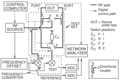
Figure \(\PageIndex{1}\): Switch-based vector network analyzer system with two receivers. The directional couplers selectively couple forward- or backward-traveling waves. With the directional coupler (see inset), a traveling wave inserted at Port \(\mathsf{2}\) appears only at Port \(\mathsf{1}\). A traveling wave inserted at Port \(\mathsf{1}\) appears at Port \(\mathsf{2}\) and a coupled version at Port \(\mathsf{3}\). A traveling wave inserted at Port \(\mathsf{3}\) appears only at Port \(\mathsf{1}\). Switch positions determine which \(S\) parameter is measured.
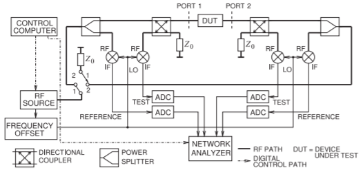
Figure \(\PageIndex{2}\): Vector network analyzer system with four receivers.
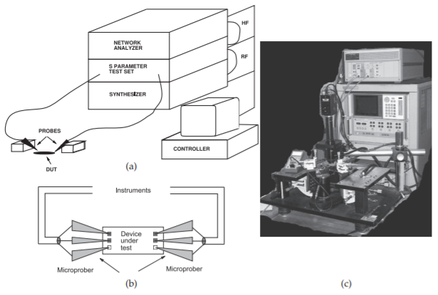
Figure \(\PageIndex{3}\): \(S\) parameter measurement system: (a) shown in a configuration to do on-chip testing; (b) details of coplanar probes with a GSG configuration and contacting pads; and (c) a vector network analyzer in the background with probe station including camera.
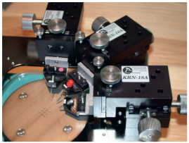
Figure \(\PageIndex{4}\): Micropositioners used with coplanar probes. Used with permission of J MicroTechnology, Inc.
Probing elements required for on-wafer measurements are shown in Figure \(\PageIndex{5}\). Figure \(\PageIndex{5}\)(a) shows a single RF probe that is essentially an extended coaxial line. Figure \(\PageIndex{5}\)(c) shows a microprobe making a connection to a transmission line on an IC and the lower image in Figure \(\PageIndex{5}\)(b) shows greater detail of the contact area.
A typical microprobe is based on a micro coaxial cable with the center conductor (carrying the signal) extended a millimeter or so to form a needlelike contact. Two other needle-like contacts are made by attaching short extensions to the outer conductor of the coaxial line on either side of the signal connection (see the top image in Figure \(\PageIndex{5}\)(b)). Such probes are called
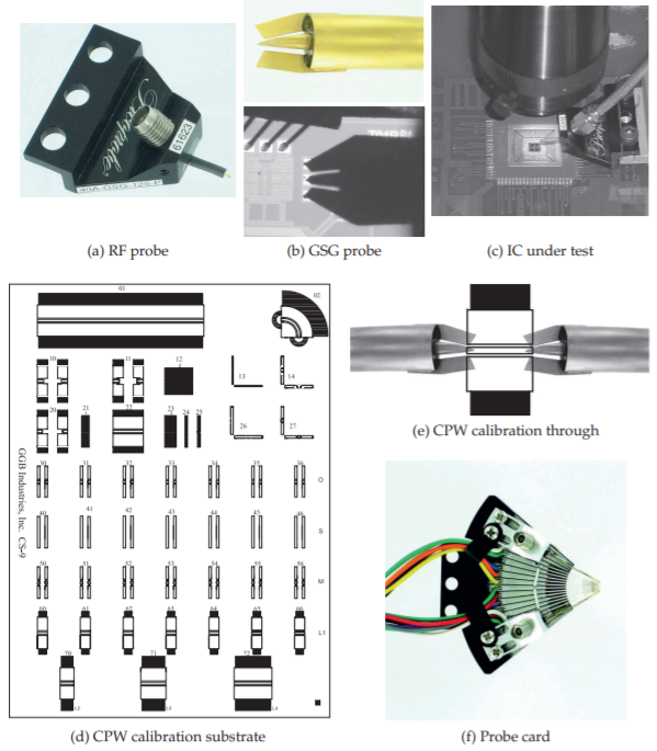
Figure \(\PageIndex{5}\): RF probes: (a) single RF probe probe; (b) detail of a GSG probe and contacting an IC; (c) an IC under test; (d) layout of a calibration substrate used with GSG probes; (e) probes contacting a through CPW structure on the calibration substrate; and (f) a probe card with 2 RF probes (top and bottom) and \(13\) needle probes for DC and low-frequency connections. ((a), (b) top, (d), (e), (f) Copyright GGB Industries Inc., used with permission [2].)
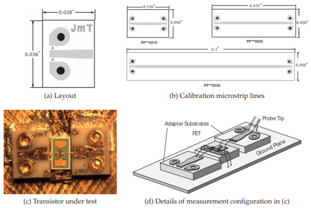
Figure \(\PageIndex{6}\): Use of a CPW-to-microstrip adaptor enabling coplanar probes to be used in characterizing a non-CPW device. The adaptors provide a low insertion loss CPW-to-microstrip transition. Used with permission of J microTechnology, Inc.
ground-signal-ground (GSG) probes and transition from a coaxial cable to an on-wafer CPW line, providing a smooth transition of the EM fields from those of a coaxial line to those of the CPW line. The on-wafer pads can be as small as \(50\:\mu\text{m}\) on a side.
Measurement using CPW probes and manipulators enables repeatable measurements to be made from DC to above \(100\text{ GHz}\). Such measurements require repeatability of probe connections that are better than \(1\:\mu\text{m}\). When the DUT has microstrip connections, it is necessary to use a CPW-to-microstrip adapter, as shown in Figure \(\PageIndex{6}\). The layout of a suitable adapter is shown in Figure \(\PageIndex{6}\)(a). In Figure \(\PageIndex{6}\)(c and d) two adaptors are shown in use in the characterization of a microwave transistor. GSG probes contact the adapters and the grounds are connected to the backside metalization by vias. Calibration uses the microstrip transmission line calibration substrates shown in Figure \(\PageIndex{6}\)(b).