
5.3: Integrated Lumped Elements
- Page ID
- 41123
\( \newcommand{\vecs}[1]{\overset { \scriptstyle \rightharpoonup} {\mathbf{#1}} } \)
\( \newcommand{\vecd}[1]{\overset{-\!-\!\rightharpoonup}{\vphantom{a}\smash {#1}}} \)
\( \newcommand{\id}{\mathrm{id}}\) \( \newcommand{\Span}{\mathrm{span}}\)
( \newcommand{\kernel}{\mathrm{null}\,}\) \( \newcommand{\range}{\mathrm{range}\,}\)
\( \newcommand{\RealPart}{\mathrm{Re}}\) \( \newcommand{\ImaginaryPart}{\mathrm{Im}}\)
\( \newcommand{\Argument}{\mathrm{Arg}}\) \( \newcommand{\norm}[1]{\| #1 \|}\)
\( \newcommand{\inner}[2]{\langle #1, #2 \rangle}\)
\( \newcommand{\Span}{\mathrm{span}}\)
\( \newcommand{\id}{\mathrm{id}}\)
\( \newcommand{\Span}{\mathrm{span}}\)
\( \newcommand{\kernel}{\mathrm{null}\,}\)
\( \newcommand{\range}{\mathrm{range}\,}\)
\( \newcommand{\RealPart}{\mathrm{Re}}\)
\( \newcommand{\ImaginaryPart}{\mathrm{Im}}\)
\( \newcommand{\Argument}{\mathrm{Arg}}\)
\( \newcommand{\norm}[1]{\| #1 \|}\)
\( \newcommand{\inner}[2]{\langle #1, #2 \rangle}\)
\( \newcommand{\Span}{\mathrm{span}}\) \( \newcommand{\AA}{\unicode[.8,0]{x212B}}\)
\( \newcommand{\vectorA}[1]{\vec{#1}} % arrow\)
\( \newcommand{\vectorAt}[1]{\vec{\text{#1}}} % arrow\)
\( \newcommand{\vectorB}[1]{\overset { \scriptstyle \rightharpoonup} {\mathbf{#1}} } \)
\( \newcommand{\vectorC}[1]{\textbf{#1}} \)
\( \newcommand{\vectorD}[1]{\overrightarrow{#1}} \)
\( \newcommand{\vectorDt}[1]{\overrightarrow{\text{#1}}} \)
\( \newcommand{\vectE}[1]{\overset{-\!-\!\rightharpoonup}{\vphantom{a}\smash{\mathbf {#1}}}} \)
\( \newcommand{\vecs}[1]{\overset { \scriptstyle \rightharpoonup} {\mathbf{#1}} } \)
\( \newcommand{\vecd}[1]{\overset{-\!-\!\rightharpoonup}{\vphantom{a}\smash {#1}}} \)
\(\newcommand{\avec}{\mathbf a}\) \(\newcommand{\bvec}{\mathbf b}\) \(\newcommand{\cvec}{\mathbf c}\) \(\newcommand{\dvec}{\mathbf d}\) \(\newcommand{\dtil}{\widetilde{\mathbf d}}\) \(\newcommand{\evec}{\mathbf e}\) \(\newcommand{\fvec}{\mathbf f}\) \(\newcommand{\nvec}{\mathbf n}\) \(\newcommand{\pvec}{\mathbf p}\) \(\newcommand{\qvec}{\mathbf q}\) \(\newcommand{\svec}{\mathbf s}\) \(\newcommand{\tvec}{\mathbf t}\) \(\newcommand{\uvec}{\mathbf u}\) \(\newcommand{\vvec}{\mathbf v}\) \(\newcommand{\wvec}{\mathbf w}\) \(\newcommand{\xvec}{\mathbf x}\) \(\newcommand{\yvec}{\mathbf y}\) \(\newcommand{\zvec}{\mathbf z}\) \(\newcommand{\rvec}{\mathbf r}\) \(\newcommand{\mvec}{\mathbf m}\) \(\newcommand{\zerovec}{\mathbf 0}\) \(\newcommand{\onevec}{\mathbf 1}\) \(\newcommand{\real}{\mathbb R}\) \(\newcommand{\twovec}[2]{\left[\begin{array}{r}#1 \\ #2 \end{array}\right]}\) \(\newcommand{\ctwovec}[2]{\left[\begin{array}{c}#1 \\ #2 \end{array}\right]}\) \(\newcommand{\threevec}[3]{\left[\begin{array}{r}#1 \\ #2 \\ #3 \end{array}\right]}\) \(\newcommand{\cthreevec}[3]{\left[\begin{array}{c}#1 \\ #2 \\ #3 \end{array}\right]}\) \(\newcommand{\fourvec}[4]{\left[\begin{array}{r}#1 \\ #2 \\ #3 \\ #4 \end{array}\right]}\) \(\newcommand{\cfourvec}[4]{\left[\begin{array}{c}#1 \\ #2 \\ #3 \\ #4 \end{array}\right]}\) \(\newcommand{\fivevec}[5]{\left[\begin{array}{r}#1 \\ #2 \\ #3 \\ #4 \\ #5 \\ \end{array}\right]}\) \(\newcommand{\cfivevec}[5]{\left[\begin{array}{c}#1 \\ #2 \\ #3 \\ #4 \\ #5 \\ \end{array}\right]}\) \(\newcommand{\mattwo}[4]{\left[\begin{array}{rr}#1 \amp #2 \\ #3 \amp #4 \\ \end{array}\right]}\) \(\newcommand{\laspan}[1]{\text{Span}\{#1\}}\) \(\newcommand{\bcal}{\cal B}\) \(\newcommand{\ccal}{\cal C}\) \(\newcommand{\scal}{\cal S}\) \(\newcommand{\wcal}{\cal W}\) \(\newcommand{\ecal}{\cal E}\) \(\newcommand{\coords}[2]{\left\{#1\right\}_{#2}}\) \(\newcommand{\gray}[1]{\color{gray}{#1}}\) \(\newcommand{\lgray}[1]{\color{lightgray}{#1}}\) \(\newcommand{\rank}{\operatorname{rank}}\) \(\newcommand{\row}{\text{Row}}\) \(\newcommand{\col}{\text{Col}}\) \(\renewcommand{\row}{\text{Row}}\) \(\newcommand{\nul}{\text{Nul}}\) \(\newcommand{\var}{\text{Var}}\) \(\newcommand{\corr}{\text{corr}}\) \(\newcommand{\len}[1]{\left|#1\right|}\) \(\newcommand{\bbar}{\overline{\bvec}}\) \(\newcommand{\bhat}{\widehat{\bvec}}\) \(\newcommand{\bperp}{\bvec^\perp}\) \(\newcommand{\xhat}{\widehat{\xvec}}\) \(\newcommand{\vhat}{\widehat{\vvec}}\) \(\newcommand{\uhat}{\widehat{\uvec}}\) \(\newcommand{\what}{\widehat{\wvec}}\) \(\newcommand{\Sighat}{\widehat{\Sigma}}\) \(\newcommand{\lt}{<}\) \(\newcommand{\gt}{>}\) \(\newcommand{\amp}{&}\) \(\definecolor{fillinmathshade}{gray}{0.9}\)This section considers lumped-elements used in integrated circuits operating at microwave frequencies. Lumped elements such as capacitors, inductors and resistors can rarely be regarded as pure elements at microwave frequencies. Inductors and capacitors have significant loss and all of the elements store energy in both electric and magnetic forms.
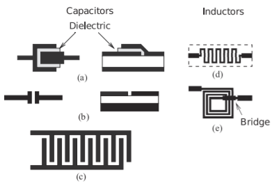
Figure \(\PageIndex{1}\): Monolithic lumped elements: (a) parallel plate capacitor; (b) gap capacitor; (c) interdigitated capacitor; (d) meander line inductor; and (e) spiral inductor.
5.3.1 On-Chip Capacitors
There are three primary forms of on-chip capacitor:
- Metal-dielectric-metal capacitor—using interconnect metalization.
- Metal-dielectric-semiconductor capacitor—essentially a MOS transistor.
- Semiconductor junction capacitor—either the capacitance of a reverse-biased \(pn\) junction or Schottky barrier.
In silicon technology it is common to refer to the first capacitor type as a metal-oxide-metal (MOM) capacitor or as a metal-insulator-metal (MIM) capacitor. A MOM capacitor can be realized as a parallel plate capacitance (see Figure \(\PageIndex{1}\)(a)), and multiple levels of metalization can be used to increase the capacitance density. Relatively low capacitance values of up to \(500\text{ fF/}\mu\text{m}^{2}\) are typically available.
An alternative MOM capacitance is available using lateral arrangements of conductors on the same layer (see Figure \(\PageIndex{1}\)(b)); that is, adjacent metal structures are separated by a small horizontal gap. Again, there are two distinct metal connections, and a smaller metal separation can be obtained using photolithography than that possible using dielectric separation. However the capacitance density is only increased by a factor of about three. Higher values can be obtained using the interdigitated capacitor (IDC) of Figure \(\PageIndex{1}\)(c). Both types of MOM capacitance, parallel plate and lateral, are geometrically defined, are voltage independent, have very low temperature coefficients, and have initial fabrication tolerances of \(20\%–30\%\).
The second type of capacitor in MOS technology is referred to as a metal-oxide-semiconductor (MOS) capacitor. MOS capacitors use a MOS transistor with a parallel-plate capacitance between the gate of a MOS transistor and a heavily inverted channel. The drain and source are connected in this configuration and the separation between the conductors is thin, being the gate oxide thickness. This leads to high values of capacitance, although with a weak voltage dependence. Junction capacitance is realized as the capacitance of a reverse-biased semiconductor junction. This capacitance can be quite large, but has a strong voltage dependence. This voltage dependence can be utilized to realize tunable circuits (e.g., a voltage-controlled oscillator).
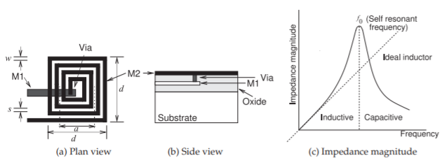
Figure \(\PageIndex{2}\): An on-chip spiral inductor.
5.3.2 Planar Inductors
Inductors are important components in RF and microwave circuits. In addition to their role in matching networks, they are used to provide bias to active devices while effectively blocking RF signals from the bias circuitry. Inductors of up to \(10\text{ nH}\) can be fabricated in compact form, with the spiral inductor of Figure \(\PageIndex{1}\)(e) being typical. Bond wires can also be used to realize small inductances in the \(0.5–1\text{ nH}\) range. One of the advantages of having a portion of a large inductance on-chip is reduced sensitivity to die attach (bondwire, etc.) connections used to connect to an external inductance. Small values of inductance can be realized by the meander line inductor of Figure \(\PageIndex{1}\)(d). This is based on a high-impedance length of line (narrow line in microstrip) appearing inductive.
An on-chip spiral inductor is shown in Figure \(\PageIndex{2}\). An approximate expression for the inductance of this structure was developed by Wheeler [1, 2, 3]:
\[\label{eq:1}L\approx\frac{9.4\mu_{0}n^{2}a^{2}}{11d-7a} \]
where \(a\) is the mean radius of the spiral and \(n\) is the number of turns. This formula was derived for circular coils, but its accuracy for square spirals is within \(5\%\) of values obtained using EM simulation [4]. It is therefore a very useful formula in the early stages of design, but EM analysis is required to obtain the necessary accuracy and frequency dependence of the inductor. Fields produced by a spiral inductor penetrate the substrate, and as the ground plane is located at a short distance away, the eddy currents on the ground plane reduce the inductance that would otherwise be obtained. The eddy current in the ground conductor rotates in a direction opposite to that of the current on the spiral itself. As a result, the flux of the image inductor in the ground is in the opposite direction to that produced by the spiral itself, with the consequent effect that the effective total inductance is reduced. By creating a broken conductor pattern, the ground inductance is largely eliminated as the eddy currents cannot flow [5].
All inductors have appreciable resistive loss of conductors, and for inductors on semiconductor substrates, loss due to induced substrate currents is
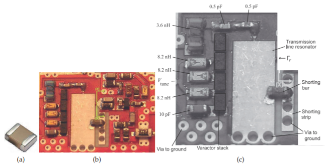
Figure \(\PageIndex{3}\): Circuit board showing the use of surface-mount components: (a) chip resistor or capacitor with metal terminals at the two ends; (b) populated RF microstrip circuit board of a \(5\text{ GHz}\) voltage-controlled oscillator [7] (the larger components have dimensions \(1.6\text{ mm}\times 0.8\text{ mm}\)); and (c) identification of several components including a varactor stack with four varactor diodes and a shorting bar that is a \(0\:\Omega\) resistor.
important and often dominates. Loss in the substrate is particularly large in silicon substrates due to the finite conductivity of the substrate and the resulting current flow. These induced currents follow a path under the conductors of the spiral and, just as with ground plane eddy currents, lowers the inductance achieved. However, the resistance of the lines is unchanged. Thus on silicon it is difficult to achieve very high \(Q_{s}\) (the ratio of stored energy to energy dissipated per cycle).
Lumped inductors are based on coils of conductor, and there is parasitic capacitance between the windings [6]. As a result there will be a frequency where the capacitance and inductance resonate at what is called the self-resonant frequency. The impedance of a realistic inductor is shown in Figure \(\PageIndex{2}\)(c). If the practical inductor was purely inductive, then its impedance would increase linearly with frequency. However, because of resonance, the effective inductance increases just before resonance causing the impedance of the practical inductor to increase more rapidly than linearly. This is seen in Figure \(\PageIndex{2}\)(c), and this effect is often used in narrowband microwave circuits.