
5.5: Terminations and Attenuators
- Page ID
- 41125
\( \newcommand{\vecs}[1]{\overset { \scriptstyle \rightharpoonup} {\mathbf{#1}} } \)
\( \newcommand{\vecd}[1]{\overset{-\!-\!\rightharpoonup}{\vphantom{a}\smash {#1}}} \)
\( \newcommand{\id}{\mathrm{id}}\) \( \newcommand{\Span}{\mathrm{span}}\)
( \newcommand{\kernel}{\mathrm{null}\,}\) \( \newcommand{\range}{\mathrm{range}\,}\)
\( \newcommand{\RealPart}{\mathrm{Re}}\) \( \newcommand{\ImaginaryPart}{\mathrm{Im}}\)
\( \newcommand{\Argument}{\mathrm{Arg}}\) \( \newcommand{\norm}[1]{\| #1 \|}\)
\( \newcommand{\inner}[2]{\langle #1, #2 \rangle}\)
\( \newcommand{\Span}{\mathrm{span}}\)
\( \newcommand{\id}{\mathrm{id}}\)
\( \newcommand{\Span}{\mathrm{span}}\)
\( \newcommand{\kernel}{\mathrm{null}\,}\)
\( \newcommand{\range}{\mathrm{range}\,}\)
\( \newcommand{\RealPart}{\mathrm{Re}}\)
\( \newcommand{\ImaginaryPart}{\mathrm{Im}}\)
\( \newcommand{\Argument}{\mathrm{Arg}}\)
\( \newcommand{\norm}[1]{\| #1 \|}\)
\( \newcommand{\inner}[2]{\langle #1, #2 \rangle}\)
\( \newcommand{\Span}{\mathrm{span}}\) \( \newcommand{\AA}{\unicode[.8,0]{x212B}}\)
\( \newcommand{\vectorA}[1]{\vec{#1}} % arrow\)
\( \newcommand{\vectorAt}[1]{\vec{\text{#1}}} % arrow\)
\( \newcommand{\vectorB}[1]{\overset { \scriptstyle \rightharpoonup} {\mathbf{#1}} } \)
\( \newcommand{\vectorC}[1]{\textbf{#1}} \)
\( \newcommand{\vectorD}[1]{\overrightarrow{#1}} \)
\( \newcommand{\vectorDt}[1]{\overrightarrow{\text{#1}}} \)
\( \newcommand{\vectE}[1]{\overset{-\!-\!\rightharpoonup}{\vphantom{a}\smash{\mathbf {#1}}}} \)
\( \newcommand{\vecs}[1]{\overset { \scriptstyle \rightharpoonup} {\mathbf{#1}} } \)
\( \newcommand{\vecd}[1]{\overset{-\!-\!\rightharpoonup}{\vphantom{a}\smash {#1}}} \)
\(\newcommand{\avec}{\mathbf a}\) \(\newcommand{\bvec}{\mathbf b}\) \(\newcommand{\cvec}{\mathbf c}\) \(\newcommand{\dvec}{\mathbf d}\) \(\newcommand{\dtil}{\widetilde{\mathbf d}}\) \(\newcommand{\evec}{\mathbf e}\) \(\newcommand{\fvec}{\mathbf f}\) \(\newcommand{\nvec}{\mathbf n}\) \(\newcommand{\pvec}{\mathbf p}\) \(\newcommand{\qvec}{\mathbf q}\) \(\newcommand{\svec}{\mathbf s}\) \(\newcommand{\tvec}{\mathbf t}\) \(\newcommand{\uvec}{\mathbf u}\) \(\newcommand{\vvec}{\mathbf v}\) \(\newcommand{\wvec}{\mathbf w}\) \(\newcommand{\xvec}{\mathbf x}\) \(\newcommand{\yvec}{\mathbf y}\) \(\newcommand{\zvec}{\mathbf z}\) \(\newcommand{\rvec}{\mathbf r}\) \(\newcommand{\mvec}{\mathbf m}\) \(\newcommand{\zerovec}{\mathbf 0}\) \(\newcommand{\onevec}{\mathbf 1}\) \(\newcommand{\real}{\mathbb R}\) \(\newcommand{\twovec}[2]{\left[\begin{array}{r}#1 \\ #2 \end{array}\right]}\) \(\newcommand{\ctwovec}[2]{\left[\begin{array}{c}#1 \\ #2 \end{array}\right]}\) \(\newcommand{\threevec}[3]{\left[\begin{array}{r}#1 \\ #2 \\ #3 \end{array}\right]}\) \(\newcommand{\cthreevec}[3]{\left[\begin{array}{c}#1 \\ #2 \\ #3 \end{array}\right]}\) \(\newcommand{\fourvec}[4]{\left[\begin{array}{r}#1 \\ #2 \\ #3 \\ #4 \end{array}\right]}\) \(\newcommand{\cfourvec}[4]{\left[\begin{array}{c}#1 \\ #2 \\ #3 \\ #4 \end{array}\right]}\) \(\newcommand{\fivevec}[5]{\left[\begin{array}{r}#1 \\ #2 \\ #3 \\ #4 \\ #5 \\ \end{array}\right]}\) \(\newcommand{\cfivevec}[5]{\left[\begin{array}{c}#1 \\ #2 \\ #3 \\ #4 \\ #5 \\ \end{array}\right]}\) \(\newcommand{\mattwo}[4]{\left[\begin{array}{rr}#1 \amp #2 \\ #3 \amp #4 \\ \end{array}\right]}\) \(\newcommand{\laspan}[1]{\text{Span}\{#1\}}\) \(\newcommand{\bcal}{\cal B}\) \(\newcommand{\ccal}{\cal C}\) \(\newcommand{\scal}{\cal S}\) \(\newcommand{\wcal}{\cal W}\) \(\newcommand{\ecal}{\cal E}\) \(\newcommand{\coords}[2]{\left\{#1\right\}_{#2}}\) \(\newcommand{\gray}[1]{\color{gray}{#1}}\) \(\newcommand{\lgray}[1]{\color{lightgray}{#1}}\) \(\newcommand{\rank}{\operatorname{rank}}\) \(\newcommand{\row}{\text{Row}}\) \(\newcommand{\col}{\text{Col}}\) \(\renewcommand{\row}{\text{Row}}\) \(\newcommand{\nul}{\text{Nul}}\) \(\newcommand{\var}{\text{Var}}\) \(\newcommand{\corr}{\text{corr}}\) \(\newcommand{\len}[1]{\left|#1\right|}\) \(\newcommand{\bbar}{\overline{\bvec}}\) \(\newcommand{\bhat}{\widehat{\bvec}}\) \(\newcommand{\bperp}{\bvec^\perp}\) \(\newcommand{\xhat}{\widehat{\xvec}}\) \(\newcommand{\vhat}{\widehat{\vvec}}\) \(\newcommand{\uhat}{\widehat{\uvec}}\) \(\newcommand{\what}{\widehat{\wvec}}\) \(\newcommand{\Sighat}{\widehat{\Sigma}}\) \(\newcommand{\lt}{<}\) \(\newcommand{\gt}{>}\) \(\newcommand{\amp}{&}\) \(\definecolor{fillinmathshade}{gray}{0.9}\)5.5.1 Terminations
Terminations are used to completely absorb a forward-traveling wave and the defining characteristic is that the reflection coefficient of a termination is ideally zero. If a transmission line has a resistive characteristic impedance
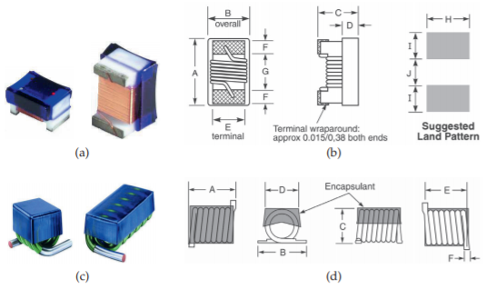
Figure \(\PageIndex{1}\): Chip inductors: (a) inductor in an 0603 surface-mount package; (b) schematic showing sizes and pads to be provided on a circuit board \((\mathsf{A}=64\text{ mils }(1.63\text{ mm}),\) \( \mathsf{B}=33\text{ mils}\: (0.84\text{ mm}),\) \(\mathsf{C}=24\text{ mils }(0.61\text{ mm}),\) \(\mathsf{D}=13\text{ mils }(0.33\text{ mm}),\) \(\mathsf{E}=30\text{ mils }(0.76\text{ mm}),\) \(\mathsf{F}=25\text{ mils }(0.64\text{ mm}),\) \(G=25\text{ mils }(0.64\text{ mm}),\) and \(\mathsf{H}=40\text{ mils }(1.02\text{ mm)});\) (c) 0201 surface-mount air-core inductor; and (d) detail \((\mathsf{A}=23\text{ mils }(0.58\text{ mm}),\) \(\mathsf{B}=18\text{ mils }(0.46\text{ mm}),\) \(\mathsf{C}=17.7\text{ mils }(0.45\text{ mm}),\) \(\mathsf{D}=4\text{ mils }(0.1\text{ mm}),\) \(\mathsf{E}=15\text{ mils }(0.38\text{ mm}),\) \(\mathsf{F}=9\text{ mils }(0.23\text{ mm}),\) \(\mathsf{G}=7\text{ mils }(0.18\text{ mm}),\) and \(\mathsf{H}=18\text{ mils }(0.46\text{ mm}))\). Copyright Coilcraft, Inc., used with permission [8].
| \(L_{\text{nom}}\) \((\text{nH})\) |
\(900\text{ MHz}\) | \(1.7\text{ GHz}\) | SRF \((\text{GHz})\) |
\(R_{\text{DC}}\) \((\Omega)\) |
\(I_{\text{max}}\) \((\text{mA})\) |
||
|---|---|---|---|---|---|---|---|
| \(L\:(\text{nH})\) | \(Q\) | \(L\:(\text{nH})\) | \(Q\) | ||||
| \(0.5\) | \(0.5\) | \(29\) | \(0.49\) | \(43\) | \(23.5\) | \(0.020\) | \(1250\) |
| \(1.2\) | \(1.16\) | \(42\) | \(1.16\) | \(60\) | \(17.9\) | \(0.042\) | \(870\) |
| \(2.3\) | \(2.28\) | \(45\) | \(2.28\) | \(64\) | \(16.5\) | \(0.070\) | \(670\) |
| \(5.2\) | \(5.21\) | \(36\) | \(5.21\) | \(55\) | \(10.0\) | \(0.170\) | \(430\) |
| \(9.6\) | \(9.62\) | \(38\) | \(9.64\) | \(53\) | \(6.2\) | \(0.400\) | \(280\) |
| \(14.0\) | \(14.13\) | \(37\) | \(14.37\) | \(51\) | \(5.1\) | \(0.440\) | \(270\) |
Table \(\PageIndex{1}\): Parameters of the inductors in Figure \(\PageIndex{1}\)(c). \(L_{\text{nom}}\) is the nominal inductance, SRF is the self-resonance frequency, RDC is the inductor’s series resistance, and \(I_{\text{max}}\) is the maximum RMS current supported.
\(R_{0} = Z_{0}\), then terminating the line in a resistance \(R_{0}\) will fully absorb the forward-traveling wave and there will be no reflection. The line is then said to be matched. At RF and microwave frequencies some refinements to this simple circuit connection are required. On a transmission line the energy is contained in the EM fields. For the coaxial line, a simple resistive connection between the inner and outer conductors would not terminate the fields and there would be some reflection. Instead, coaxial line terminations generally comprise a disk of resistive material (see Figure \(\PageIndex{2}\)(a)). The total resistance of the disk from the inner to the outer conductor is the characteristic resistance of the line, however, the resistive material is distributed and so creates a good termination of the fields guided by the coaxial conductors.
| Component | Symbol | Alternate |
|---|---|---|
| Attenuator, fixed |  |
|
| Attenuator, balanced |  |
 |
| Attenuator, unbalanced |  |
 |
| Attenuator, variable |  |
|
| Attenuator, continuously variable |  |
|
| Attenuator, stepped variable |  |
Table \(\PageIndex{2}\): IEEE standard symbols for attenuators [9].
frequencies above a few gigahertz. A high-quality termination is realized using a section of lossy line as shown in Figure \(\PageIndex{2}\)(b). Here lossy material is deposited on top of an open-circuited microstrip line. This increases the loss of the line appreciably without significantly affecting the characteristic impedance of the line. If the length of the lossy line is sufficiently long, say one wavelength, the forward-traveling wave will be totally absorbed and there will be no reflection. Tapering the lossy material, as shown in Figure \(\PageIndex{2}\)(b), reduces the discontinuity between the lossless microstrip line and the lossy line by ensuring that some of the power in the forward-traveling wave is dissipated before the maximum impact of the lossy material occurs. Thus a matched termination is achieved without the use of a via.
5.5.2 Attenuators
An attenuator is a two-port network used to reduce the amplitude of a signal and it does this by absorbing power and without distorting the signal. The input and output of the attenuator are both matched, so there are no reflections. An attenuator may be fixed, continuously variable, or discretely variable. The IEEE standard symbols for attenuators are shown in Table \(\PageIndex{2}\). When the attenuation is fixed, an attenuator is commonly called a pad. Resistive pads can be used to minimize the effect of shorts and opens on
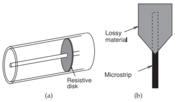
Figure \(\PageIndex{2}\): Terminations: (a) coaxial line resistive termination; (b) microstrip matched load.
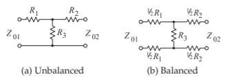
Figure \(\PageIndex{3}\): T (Tee) attenuator. \(K\) is the (power) attenuation factor, e.g. a \(3\text{ dB}\) attenuator has \(K = 10^{3/10} = 1.995\).
\[\begin{align} R_{1}&=\frac{Z_{01}(K+1)-2\sqrt{KZ_{01}Z_{02}}}{K-1}\quad R_{2}=\frac{Z_{02}(K+1)-2\sqrt{KZ_{01}Z_{02}}}{K-1}\nonumber \\ \label{eq:1}R_{3}&=\frac{2\sqrt{KZ_{01}Z_{02}}}{K-1}\end{align} \]
If \(Z_{01}=Z_{02}=Z_{0}\), then
\[\label{eq:2} R_{1}=R_{2}=Z_{0}\left(\frac{\sqrt{K}-1}{\sqrt{K}+1}\right)\quad\text{and}\quad R_{3}=\frac{2Z_{0}\sqrt{K}}{K-1} \]
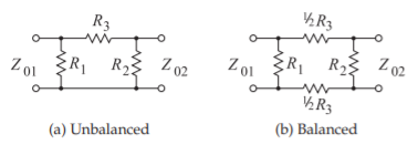
Figure \(\PageIndex{4}\): Pi (Π) attenuator. \(K\) is the (power) attenuation factor, e.g. a \(20\text{ dB}\) attenuator has \(K = 10^{20/10} = 100\).
\[\begin{align} \label{eq:3}R_{1}&=\frac{Z_{01}(K-1)\sqrt{Z_{02}}}{(K+1)\sqrt{Z_{02}}-2\sqrt{KZ_{01}}}\quad R_{2}=\frac{Z_{02}(K-1)\sqrt{Z_{01}}}{(K+1)\sqrt{Z_{01}}-2\sqrt{KZ_{02}}}\\ \label{eq:4}R_{3}&=\frac{(K-1)}{2}\sqrt{\frac{Z_{01}Z_{02}}{K}}\end{align} \]
If \(Z_{01}=Z_{02}=Z_{0}\), then
\[\label{eq:5}R_{1}=R_{2}=Z_{0}\left(\frac{\sqrt{K}+1}{\sqrt{K}-1}\right)\quad\text{and}\quad R_{3}=\frac{Z_{0}(K-1)}{2\sqrt{K}} \]
If \(R_{1}=R_{2}\), then \(Z_{01}=Z_{02}=Z_{0}\)
\[\label{eq:6}Z_{0}=\sqrt{\frac{R_{1}^{2}R_{3}}{2R_{1}+R_{3}}}\quad\text{and}\quad K=\left(\frac{R_{1}+Z_{0}}{R_{1}-Z_{0}}\right)^{2} \]
the integrity of an RF circuit. An example of attenuator use in this situation is in a cable TV system, where it is critical that the integrity of the system is not compromised by a consumer disconnecting appliances from a cable outlet.
Balanced and unbalanced resistive pads are shown in Figures \(\PageIndex{3}\) and \(\PageIndex{4}\) together with their design equations. The attenuators in Figure \(\PageIndex{3}\) are \(\text{T}\) or \(\text{Tee}\) attenuators, where \(Z_{01}\) is the system impedance to the left of the pad and \(Z_{02}\) is the system impedance to the right of the pad. The defining characteristic is that the reflection coefficient looking into the pad from the left is zero when referred to \(Z_{01}\). Similarly, the reflection coefficient looking
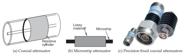
Figure \(\PageIndex{5}\): Distributed attenuators. The attenuators in (c) have power handling ratings of \(2\text{ W},\: 5\text{ W}\) and \(20\text{ W}\) (left to right). Copyright 2012 Scientific Components Corporation d/b/a MiniCircuits, used with permission [11].
from the right of the pad is zero with respect to \(Z_{02}\). The attenuation factor is
\[\label{eq:7}K=\frac{\text{Power in}}{\text{Power out}} \]
In decibels, the attenuation is
\[\label{eq:8}K|_{\text{dB}}=10\log_{10}K=(\text{Power in})|_{\text{dBm}}-(\text{Power out})|_{\text{dBm}} \]
If the left and right system impedances are different, then there is a minimum attenuation factor that can be achieved [10]:
\[\label{eq:9}K_{\text{MIN}}=\left\{\begin{array}{ll}{\left[2Z_{01}-Z_{02}+2\sqrt{Z_{01}(Z_{01}-Z_{02})}\right]/Z_{02},}&{Z_{01}\geq Z_{02}}\\{\left[2Z_{02}-Z_{01}+2\sqrt{Z_{02}(Z_{02}-Z_{01})}\right]/Z_{01},}&{Z_{01}\leq Z_{02}}\end{array}\right. \]
This limitation comes from the simultaneous requirement that the pad be matched. If there is a single system impedance, \(Z_{0} = Z_{01} = Z_{02}\), then \(K_{\text{MIN}} = 1\), and so any value of attenuation can be obtained.
Lumped attenuators are useful up to 10 GHz above which the size of resistive elements becomes large compared to a wavelength. Also, for planar circuits, vias are required, and these are undesirable from a manufacturing standpoint, and electrically they have a small inductance. Fortunately attenuators can be realized using a lossy section of transmission line, as shown in Figure \(\PageIndex{5}\). Here, lossy material results in a section of line with a high-attenuation constant. Generally the lossy material has little effect on the characteristic impedance of the line, so there is little reflection at the input and output of the attenuator. Distributed attenuators can be used at frequencies higher than lumped-element attenuators can, and they can be realized with any transmission line structure.
Another example of the use of attenuators in combining the output of two sources is shown in Figure \(\PageIndex{6}\). This is a common situation in measurements where the outputs of two instrumentation sources are to be combined. The attenuators reduce the level of the signal presented to the output of one source by the other. If the level of the second signal is high, most sources would produce nonlinear distortion, including nonlinear mixing products.
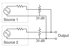
Figure \(\PageIndex{6}\): The use of attenuators to isolate the outputs of two sources that are combined.
Example \(\PageIndex{1}\): Pad Design
Design an unbalanced \(20\text{ dB}\) pad in a \(75\:\Omega\) system.
Solution
There are two possible designs using resistive pads. These are the unbalanced Tee and Pi pads shown in Figures \(\PageIndex{3}\) and \(\PageIndex{4}\). The Tee design will be chosen. The \(K\) factor is
\[\label{eq:10}K=10^{(K|_{\text{dB}}/10)} = 10^{(20/10)} = 100 \]
Since \(Z_{01} = Z_{02} = 75\:\Omega\), Equation \(\eqref{eq:2}\) yields
\[\begin{align}\label{eq:11}R_{1}&=R_{2}=75\left(\frac{\sqrt{100}-1}{\sqrt{100}+1}\right)=75\left(\frac{9}{11}\right)=61.4\:\Omega \\ \label{eq:12}R_{3}&=\frac{2\cdot 75\sqrt{100}}{100-1}=150\left(\frac{10}{99}\right)=15.2\:\Omega\end{align} \]
The final design is
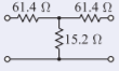
Figure \(\PageIndex{7}\)