
6.12: Exercises
- Page ID
- 41132
\( \newcommand{\vecs}[1]{\overset { \scriptstyle \rightharpoonup} {\mathbf{#1}} } \)
\( \newcommand{\vecd}[1]{\overset{-\!-\!\rightharpoonup}{\vphantom{a}\smash {#1}}} \)
\( \newcommand{\dsum}{\displaystyle\sum\limits} \)
\( \newcommand{\dint}{\displaystyle\int\limits} \)
\( \newcommand{\dlim}{\displaystyle\lim\limits} \)
\( \newcommand{\id}{\mathrm{id}}\) \( \newcommand{\Span}{\mathrm{span}}\)
( \newcommand{\kernel}{\mathrm{null}\,}\) \( \newcommand{\range}{\mathrm{range}\,}\)
\( \newcommand{\RealPart}{\mathrm{Re}}\) \( \newcommand{\ImaginaryPart}{\mathrm{Im}}\)
\( \newcommand{\Argument}{\mathrm{Arg}}\) \( \newcommand{\norm}[1]{\| #1 \|}\)
\( \newcommand{\inner}[2]{\langle #1, #2 \rangle}\)
\( \newcommand{\Span}{\mathrm{span}}\)
\( \newcommand{\id}{\mathrm{id}}\)
\( \newcommand{\Span}{\mathrm{span}}\)
\( \newcommand{\kernel}{\mathrm{null}\,}\)
\( \newcommand{\range}{\mathrm{range}\,}\)
\( \newcommand{\RealPart}{\mathrm{Re}}\)
\( \newcommand{\ImaginaryPart}{\mathrm{Im}}\)
\( \newcommand{\Argument}{\mathrm{Arg}}\)
\( \newcommand{\norm}[1]{\| #1 \|}\)
\( \newcommand{\inner}[2]{\langle #1, #2 \rangle}\)
\( \newcommand{\Span}{\mathrm{span}}\) \( \newcommand{\AA}{\unicode[.8,0]{x212B}}\)
\( \newcommand{\vectorA}[1]{\vec{#1}} % arrow\)
\( \newcommand{\vectorAt}[1]{\vec{\text{#1}}} % arrow\)
\( \newcommand{\vectorB}[1]{\overset { \scriptstyle \rightharpoonup} {\mathbf{#1}} } \)
\( \newcommand{\vectorC}[1]{\textbf{#1}} \)
\( \newcommand{\vectorD}[1]{\overrightarrow{#1}} \)
\( \newcommand{\vectorDt}[1]{\overrightarrow{\text{#1}}} \)
\( \newcommand{\vectE}[1]{\overset{-\!-\!\rightharpoonup}{\vphantom{a}\smash{\mathbf {#1}}}} \)
\( \newcommand{\vecs}[1]{\overset { \scriptstyle \rightharpoonup} {\mathbf{#1}} } \)
\(\newcommand{\longvect}{\overrightarrow}\)
\( \newcommand{\vecd}[1]{\overset{-\!-\!\rightharpoonup}{\vphantom{a}\smash {#1}}} \)
\(\newcommand{\avec}{\mathbf a}\) \(\newcommand{\bvec}{\mathbf b}\) \(\newcommand{\cvec}{\mathbf c}\) \(\newcommand{\dvec}{\mathbf d}\) \(\newcommand{\dtil}{\widetilde{\mathbf d}}\) \(\newcommand{\evec}{\mathbf e}\) \(\newcommand{\fvec}{\mathbf f}\) \(\newcommand{\nvec}{\mathbf n}\) \(\newcommand{\pvec}{\mathbf p}\) \(\newcommand{\qvec}{\mathbf q}\) \(\newcommand{\svec}{\mathbf s}\) \(\newcommand{\tvec}{\mathbf t}\) \(\newcommand{\uvec}{\mathbf u}\) \(\newcommand{\vvec}{\mathbf v}\) \(\newcommand{\wvec}{\mathbf w}\) \(\newcommand{\xvec}{\mathbf x}\) \(\newcommand{\yvec}{\mathbf y}\) \(\newcommand{\zvec}{\mathbf z}\) \(\newcommand{\rvec}{\mathbf r}\) \(\newcommand{\mvec}{\mathbf m}\) \(\newcommand{\zerovec}{\mathbf 0}\) \(\newcommand{\onevec}{\mathbf 1}\) \(\newcommand{\real}{\mathbb R}\) \(\newcommand{\twovec}[2]{\left[\begin{array}{r}#1 \\ #2 \end{array}\right]}\) \(\newcommand{\ctwovec}[2]{\left[\begin{array}{c}#1 \\ #2 \end{array}\right]}\) \(\newcommand{\threevec}[3]{\left[\begin{array}{r}#1 \\ #2 \\ #3 \end{array}\right]}\) \(\newcommand{\cthreevec}[3]{\left[\begin{array}{c}#1 \\ #2 \\ #3 \end{array}\right]}\) \(\newcommand{\fourvec}[4]{\left[\begin{array}{r}#1 \\ #2 \\ #3 \\ #4 \end{array}\right]}\) \(\newcommand{\cfourvec}[4]{\left[\begin{array}{c}#1 \\ #2 \\ #3 \\ #4 \end{array}\right]}\) \(\newcommand{\fivevec}[5]{\left[\begin{array}{r}#1 \\ #2 \\ #3 \\ #4 \\ #5 \\ \end{array}\right]}\) \(\newcommand{\cfivevec}[5]{\left[\begin{array}{c}#1 \\ #2 \\ #3 \\ #4 \\ #5 \\ \end{array}\right]}\) \(\newcommand{\mattwo}[4]{\left[\begin{array}{rr}#1 \amp #2 \\ #3 \amp #4 \\ \end{array}\right]}\) \(\newcommand{\laspan}[1]{\text{Span}\{#1\}}\) \(\newcommand{\bcal}{\cal B}\) \(\newcommand{\ccal}{\cal C}\) \(\newcommand{\scal}{\cal S}\) \(\newcommand{\wcal}{\cal W}\) \(\newcommand{\ecal}{\cal E}\) \(\newcommand{\coords}[2]{\left\{#1\right\}_{#2}}\) \(\newcommand{\gray}[1]{\color{gray}{#1}}\) \(\newcommand{\lgray}[1]{\color{lightgray}{#1}}\) \(\newcommand{\rank}{\operatorname{rank}}\) \(\newcommand{\row}{\text{Row}}\) \(\newcommand{\col}{\text{Col}}\) \(\renewcommand{\row}{\text{Row}}\) \(\newcommand{\nul}{\text{Nul}}\) \(\newcommand{\var}{\text{Var}}\) \(\newcommand{\corr}{\text{corr}}\) \(\newcommand{\len}[1]{\left|#1\right|}\) \(\newcommand{\bbar}{\overline{\bvec}}\) \(\newcommand{\bhat}{\widehat{\bvec}}\) \(\newcommand{\bperp}{\bvec^\perp}\) \(\newcommand{\xhat}{\widehat{\xvec}}\) \(\newcommand{\vhat}{\widehat{\vvec}}\) \(\newcommand{\uhat}{\widehat{\uvec}}\) \(\newcommand{\what}{\widehat{\wvec}}\) \(\newcommand{\Sighat}{\widehat{\Sigma}}\) \(\newcommand{\lt}{<}\) \(\newcommand{\gt}{>}\) \(\newcommand{\amp}{&}\) \(\definecolor{fillinmathshade}{gray}{0.9}\)- Consider the design of a magnetic transformer that will match the \(3\:\Omega\) output resistance of a power amplifier (this is the source) to a \(50\:\Omega\) load. The secondary of the transformer is on the load side.
- What is the ratio of the number of primary turns to the number of secondary turns for ideal matching?
- If the transformer ratio could be implemented exactly (the ideal situation), what is the reflection coefficient normalized to \(3\:\Omega\) looking into the primary of the transformer with the \(50\:\Omega\) load?
- What is the ideal return loss of the loaded transformer (looking into the primary)? Express your answer in \(\text{dB}\).
- If there are \(100\) secondary windings, how many primary windings are there in your design? Note that the number of windings must be an integer. (This practical situation will be considered in the rest of the problem.)
- What is the input resistance of the transformer looking into the primary?
- What is the reflection coefficient normalized to \(3\:\Omega\) looking into the primary of the transformer with the \(50\:\Omega\) load?
- What is the actual return loss (in \(\text{dB}\)) of the loaded transformer (looking into the primary)?
- If the maximum available power from the amplifier is \(20\text{ dBm}\), how much power (in \(\text{dBm}\)) is reflected at the input of the transformer?
- Thus, how much power (in \(\text{dBm}\)) is delivered to the load ignoring loss in the transformer?
- Consider the design of a magnetic transformer that will match a \(50\:\Omega\) output resistance to the \(100\:\Omega\) load presented by an amplifier. The secondary of the transformer is on the load (amplifier) side.
- What is the ratio of the number of primary turns to the number of secondary turns for ideal matching?
- If the transformer ratio could be implemented exactly (the ideal situation), what is the reflection coefficient normalized to \(50\:\Omega\) looking into the primary of the transformer with the load?
- What is the ideal return loss of the loaded transformer (looking into the primary)? Express your answer in \(\text{dB}\).
- If there are \(20\) secondary windings, how many primary windings are there in your design? Note that the number of windings must be an integer? (This situation will be considered in the rest of the problem.)
- What is the input resistance of the transformer looking into the primary?
- What is the reflection coefficient normalized to \(50\:\Omega\) looking into the primary of the loaded transformer?
- What is the actual return loss (in \(\text{dB}\)) of the loaded transformer (looking into the primary)?
- If the maximum available power from the source is \(−10\text{ dBm}\), how much power (in \(\text{dBm}\)) is reflected from the input of the transformer?
- Thus, how much power (in \(\text{dBm}\)) is delivered to the amplifier ignoring loss in the transformer?
- Consider the design of an \(\text{L}\)-matching network centered at \(1\text{ GHz}\) that will match the \(2\:\Omega\) output resistance of a power amplifier (this is the source) to a \(50\:\Omega\) load. [Parallels Example 6.4.1 but note the DC blocking requirement below.]
- What is the \(Q\) of the matching network?
- The matching network must block DC current. Draw the topology of the matching network.
- What is the reactance of the series element in the matching network?
- What is the reactance of the shunt element in the matching network?
- What is the value of the series element in the matching network?
- What is the value of the shunt element in the matching network?
- Draw and label the final design of your matching network including the source and load resistances.
- Approximately, what is the \(3\text{ dB}\) bandwidth of the matching network?
- Consider the design of an \(\text{L}\)-matching network centered at \(100\text{ GHz}\) that will match a source with a Thevenin resistance of \(50\:\Omega\) to the input of an amplifier presenting a load resistance of \(100\:\Omega\) to the matching network. [Parallels Example 6.4.2 but note the DC blocking requirement below.]
- What is the \(Q\) of the matching network?
- The matching network must block DC current. Draw the topology of the matching network.
- What is the reactance of the series element in the matching network?
- What is the reactance of the shunt element in the matching network?
- What is the value of the series element in the matching network?
- What is the value of the shunt element in the matching network?
- Draw and label the final design of your matching network including the source and load resistance.
- Approximately, what is the \(3\text{ dB}\) bandwidth of the matching network?
- Design a Pi network to match the source configuration to the load configuration below. The design frequency is \(900\text{ MHz}\) and the desired \(Q\) is \(10\). [Parallels Example 6.6.2]
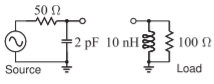
Figure \(\PageIndex{1}\)
- Design a Pi network to match the source configuration to the load configuration below. The design frequency is \(900\text{ MHz}\) and the desired \(Q\) is \(10\). [Parallels Example 6.6.2]
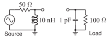
Figure \(\PageIndex{2}\)
- Develop the electrical design of an \(\text{L}\)-matching network to match the source to the load below.
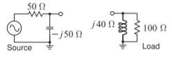
Figure \(\PageIndex{3}\)
- Develop the electrical design of an \(\text{L}\)-matching network to match the source to the load below.
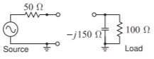
Figure \(\PageIndex{4}\)
- Design a lowpass lumped-element matching network to match the source and load shown below. The design frequency is \(1\text{ GHz}\). You must use a Smith Chart and clearly show your working and derivations. You must develop the final values of the elements.
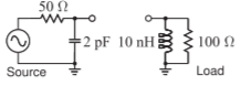
Figure \(\PageIndex{5}\)
- Consider the design of an \(\text{L}\)-matching network centered at \(100\text{ GHz}\) that will match a source with a Thevenin resistance of \(50\:\Omega\) to the input of an amplifier presenting a load resistance of \(200\:\Omega\) to the matching network. [Parallels Example 6.4.2 but note the DC blocking requirement below.]
- What is the \(Q\) of the matching network?
- The matching network must block DC current. Draw the topology of the matching network.
- What is the reactance of the series element in the matching network?
- What is the reactance of the shunt element in the matching network?
- What is the value of the series element in the matching network?
- What is the value of the shunt element in the matching network?
- Draw and label the final design of your matching network including the source and load resistance.
- Approximately, what is the \(3\text{ dB}\) bandwidth of the matching network?
- Consider the design of the output matching network of a \(15\text{ GHz}\) small-signal amplifier. The amplifier consists of an active two-port and input and output matching networks. Port \(\mathsf{1}\) is the input of the active device and Port \(\mathsf{2}\) is its output, and its \(50\:\Omega\: S\) parameters are \(S_{11} = 0.5\angle 45^{\circ},\: S_{12} = 0.1\angle 0^{\circ},\: S_{21} = 2\angle 90^{\circ},\) and \(S_{22} = 0.75\angle − 45^{\circ}\).
- If the input of the active device is terminated in \(50\:\Omega\), what is the impedance looking into the output of the amplifier?
- Design a two-element lumped-element matching network for maximum power transfer from the output of the transistor into a \(50\:\Omega\) load. Develop at least two designs and compare them. (Note that the output of the active device physically appears as a resistance in parallel with a capacitance and this can be used in contrasting your designs.)
- Develop a two-element matching network for the source/load configuration shown in the figure below. The matching network must pass DC. The center frequency of the matching network is \(f = 1\text{ GHz}\). There are a number of design considerations that should be considered before embarking on network synthesis.
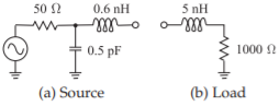
Figure \(\PageIndex{6}\)
Consider the following:
- The source needs to be collapsed to an equivalent circuit with one resistance and one reactance.
- The reactive elements in the source and the load will be accommodated using absorption or resonance. Absorption is preferred, but not always possible.
- The DC requirements necessitate a lowpass matching network. So there must be a series inductance and a shunt capacitor in the matching network. Since the load resistance is greater than the source resistance, the most likely design has a shunt capacitor on the load side. However, this may change when the transforming properties of the source and load reactances are considered.
- The source reactance should be handled by a series inductor or a shunt capacitor. The input impedance of the source must be considered to determine which.
- The load reactance will be resonated out by a shunt capacitor. Looks like absorption will be a possibility at the load.
- What is the input impedance of the source? Treat the voltage generator as a short circuit.
- What is the reactance of the series element that will resonate the effective input reactance of the source?
- What is the input admittance of the load?
- What is the shunt reactance required to resonate the load?
- What is the resistive matching problem? That is, since the reactances of the load and source have been resonated out of consideration, what are the effective source and load resistances. Derive the required matching network. Keep the element values of the matching network as reactances.
- Draw the complete matching network showing source and load elements required for resonance as well as the matching network for the resistive problem. Keep the element values as reactances.
- Draw the final matching network combining all resonant and matching elements. Keep the element values as reactances. This is the electrical design of the matching network.
- Calculate the inductance and capacitance values of the matching network.
- Design a two-element matching network to interface a source with a \(25\:\Omega\) Thevenin equivalent impedance to a load consisting of a capacitor in parallel with a resistor so that the load admittance is \(Y_{L} = 0.02 +\jmath 0.02\: S\). Use the absorption method to handle the reactive load.
- Design a matching network to interface a source with a \(25\:\Omega\) Thevenin equivalent impedance to a load consisting of a capacitor in parallel with a resistor so that the load admittance is \(Y_{L} = 0.01 +\jmath 0.01\: S\).
- If the complexity of the matching network is not limited, what is the minimum \(Q\) that could possibly be achieved in the complete network consisting of the matching network and the source and load impedances?
- Outline the procedure for designing the matching network for maximum bandwidth if only four elements can be used in the network. You do not need to design the network.
- Design a lumped-element matching network to match a source, with a Thevenin equivalent impedance of \(50\:\Omega\), to a load that consists of a \(100\:\Omega\) resistor in parallel with a \(5\text{ pF}\) capacitor. Design the matching network for maximum bandwidth at \(1\text{ GHz}\) using no more than four lumped elements.
- How many elements are there in the matching network?
- Outline how you will design the matching network.
- Design the matching network. You must draw the final design, including the source and load elements, and label each of the lumped elements using reactance values. (That is, do not calculate values of the inductance and capacitances in your design.) (Do not use a Smith chart.)
- The output of a transistor amplifier is modeled as a current source in parallel with both a \(50\:\Omega\) resistor and a \(1\text{ pF}\) capacitor. This is to be matched to a load consisting of a \(25\:\Omega\) resistor in series with a \(0.02\text{ nH}\) inductor. The task is to design a matching network that will enable DC bias to be applied from the load to the transistor output, thus the matching network must be a lowpass type. The center frequency of the system is \(10\text{ GHz}\) and a bandwidth of \(50\text{ MHz}\) is required.
- What is the fractional bandwidth of the system?
- What is the \(Q\) of the system?
- Indicate the form of the matching network if no more than four reactive elements are to be used; that is, sketch the matching network.
- Complete the design of the amplifier providing numerical element values.
- Design a Pi network to match the source configuration to the load configuration below. The design frequency is \(900\text{ MHz}\) and the desired \(Q\) is \(10\).
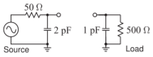
Figure \(\PageIndex{7}\)
- Design a passive matching network that will achieve maximum bandwidth matching from a source with an impedance of \(2\:\Omega\) (typical of the output impedance of a power amplifier) to a load with an impedance of \(50\:\Omega\). The matching network can have a maximum of three reactive elements. You need only calculate reactances and not the capacitor and inductor values.
- Design a passive matching network that will achieve maximum bandwidth matching from a source with an impedance of \(20\:\Omega\) to a load with an impedance of \(125\:\Omega\). The matching network can have a maximum of four reactive elements. You need only calculate reactances and not the capacitor and inductor values.
- Will you use two, three, or four elements in your matching network?
- With a diagram, and perhaps equations, indicate the design procedure.
- Design the matching network. It is sufficient to use reactance values.
- Design a passive matching network that will achieve maximum bandwidth matching from a source with an impedance of \(60\:\Omega\) to a load with an impedance of \(5\:\Omega\). The matching network can have a maximum of four reactive elements. You need only calculate reactances and not the capacitor and inductor values.
- Will you use two, three, or four elements in your matching network?
- With a diagram and perhaps equations, indicate the design procedure.
- Design the matching network. It is sufficient to use reactance values.
- Design a \(\text{T}\) network to match a \(50\:\Omega\) source to a \(1000\:\Omega\) load. The desired loaded \(Q\) is \(15\).
- Repeat Example 6.3.2 with an inductor in series with the load. Show that the inductance can be adjusted to obtain any positive shunt resistance value.
- Design a three-lumped-element matching network that interfaces a source with an impedance of \(5\:\Omega\) to a load with an impedance consisting of a resistor with an impedance of \(10\:\Omega\). The network must have a \(Q\) of \(6\).
- A source with a Thevenin equivalent impedance of \(75\:\Omega\) must drive a load with an impedance of \(5\:\Omega\). A matching network with maximum possible bandwidth between the source and the load must be designed to achieve maximum power transfer. Design the matching network for maximum possible bandwidth using no more than four reactive elements.
- Sketch the schematic of the matching network.
- Describe the design procedure.
- Complete the design of the matching network. Determine the values of the elements if the center frequency is \(1\text{ GHz}\).
- A two-port matching network is shown below with a generator and a load. The generator impedance is 40 Ω and the load impedance is \(Z_{L} = 50 −\jmath 20\:\Omega\). Use a Smith chart to design the matching network.
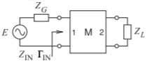
Figure \(\PageIndex{8}\)
- What is the condition for maximum power transfer from the generator? Express your answer using impedances.
- What is the condition for maximum power transfer from the generator? Express your answer using reflection coefficients.
- What system reference impedance are you going to use to solve the problem?
- Plot \(Z_{L}\) on the Smith chart and label the point. (Remember to use impedance normalization if required.)
- Plot \(Z_{G}\) on the Smith chart and label the point.
- Design a matching network using only transmission lines. Show your work on the Smith chart. You must express the lengths of the lines in terms of electrical length (either degrees or wavelengths). Characteristic impedances of the lines are required. (You will therefore have a design that consists of one stub and one other length of transmission line.)
- A two-port matching network is shown below with a generator and a load. The generator impedance is \(60\:\Omega\) and the load impedance is \(Z_{L} = 30 + \jmath 30\:\Omega\). Use a Smith chart to design a lossless matching network. It is important that your solution can be followed, so you must indicate your solution clearly on the chart.
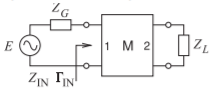
Figure \(\PageIndex{9}\)
- What is the condition for maximum power transfer from the generator? Express your answer using impedances.
- What is the condition for maximum power transfer from the generator? Express your answer using reflection coefficients.
- What system reference impedance are you going to use to solve the problem?
- Plot \(Z_{L}\) on the Smith chart and label the point. (Remember to use impedance normalization if required.)
- Plot \(Z_{G}\) on the Smith chart and label the point.
- Design a lossless lumped-element matching network showing your design process on the Smith chart. Label critical points on the Smith chart. Draw the matching network and show the reactance values.
- A two-port matching network is shown below with a generator and a load. The generator impedance is \(30\:\Omega\) and the load impedance is \(Z_{L} = 90 −\jmath 30\:\Omega\). Use a Smith chart to design a lossless matching network.
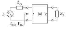
Figure \(\PageIndex{10}\)
- What is the condition for maximum power transfer from the generator? Express your answer using impedances.
- What is the condition for maximum power transfer from the generator? Express your answer using reflection coefficients.
- What system reference impedance are you going to use to solve the problem?
- Plot \(Z_{L}\) on the Smith chart and label the point. (Remember to use impedance normalization if required.)
- Plot \(Z_{G}\) on the Smith chart and label the point.
- Design a lossless matching network showing your design process on the Smith chart. Label critical points on the Smith chart. Draw the matching network and show the reactance values.
- Use Smith chart techniques to design a double-stub matching network to match a load with a normalized admittance \(y_{L} = 0.7−\jmath 5\) to a source with a normalized admittance of \(1\). The stubs are short-circuited and are separated by a transmission line of length \(\lambda /8\). The load is at the position of the first stub. All transmission lines have the system characteristic impedance. Your design should yield the lengths of the two stubs.
- Plot the load on a Smith chart. Clearly indicate the load.
- Determine the admittances of each of the stubs. Clearly show and describe your design technique so that it can be understood. Label your efforts on a Smith chart and describe the design steps. Note that a description is required and not simply markings on a Smith chart.
- Determine the electrical lengths of the stubs (express your answer in terms of wavelengths or degrees).
- Use a lossless transmission line and a series reactive element to match a source with a Thevenin equivalent impedance of \(25 + \jmath 50\:\Omega\) to a load of \(100\:\Omega\). (That is, use one transmission line and one series reactance only.)
- Draw the matching network with the source and load.
- What is the value of the series reactance in the matching network (you can leave this in ohms)?
- What is the length and characteristic impedance of the transmission line?
- Consider a load \(Z_{L} = 100 −\jmath 150\:\Omega\). Use the Smith chart to design a two-stub matching network that will match the load to a \(50\:\Omega\) generator. Use \(50\:\Omega\) transmission lines throughout and assume that the load is immediately next to the first stub. The two stubs are separated by a line with an electrical length of \(45^{\circ}\). Both stubs are short-circuited.
- Draw the matching stub system.
- What is the normalized load impedance?
- Briefly indicate the procedure used to design the two-stub matching network. You will need to use stylized Smith charts.
- Plot the load on a Smith chart.
- What is the admittance of the first stub (Stub \(1\))?
- What is the electrical length of Stub \(1\)? (Note that the stub is short circuited.)
- What is the admittance of the second stub near the generator (Stub \(2\))?
- What is the electrical length of Stub \(2\)? (Note that the stub is short circuited.)
- Consider a load \(Z_{L} = 80 +\jmath 40\:\Omega\). Use the Smith chart to design a matching network consisting of only two transmission lines that will match the load to a generator of \(40\:\Omega\).
- Draw the matching network with transmission lines. If you use a stub, it should be a short-circuited stub.
- Indicate your choice of characteristic impedance for your transmission lines. What is the normalized load impedance? What is the normalized source impedance?
- Briefly outline the design procedure you will use. You will need to use Smith chart sketches.
- Plot the load and source on a Smith chart.
- Complete the design of the matching network, providing the lengths of the transmission lines.
- A two-port matching network is shown below with a generator and a load. The generator impedance is \(40\:\Omega\) and the load impedance is \(Z_{L} = 20 −\jmath 50\:\Omega\). Use a Smith chart to design the matching network.
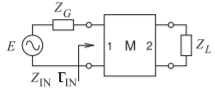
Figure \(\PageIndex{11}\)
- What is the condition for maximum power transfer from the generator? Express your answer using impedances.
- What is the condition for maximum power transfer from the generator? Express your answer using reflection coefficients.
- What system reference impedance are you going to use to solve the problem?
- Plot \(Z_{L}\) on a Smith chart and label the point. (Remember to use impedance normalization if required.)
- Plot \(Z_{G}\) on a Smith chart and label the point.
- Design a matching network using only transmission lines and show your work on a Smith chart. You must express the lengths of the lines in terms of electrical length (either degrees or wavelengths long). Characteristic impedances of the lines are required. (You will therefore have a design that consists of one stub and one other length of transmission line.)
- Use a Smith chart to design a microstrip network to match a load \(Z_{L} = 10 −\jmath 30\:\Omega\) to a source \(Z_{S} = 60 +\jmath 40\:\Omega\). Use a substrate with permittivity \(\varepsilon_{r} = 10.0\) and thickness \(500\:\mu\text{m}\).
- What is the condition for maximum power transfer?
- Develop the electrical design of the matching network using the Smith chart using \(50\:\Omega\) lines only.
- Develop the full physical design of the matching network. Draw the microstrip layout and label critical dimensions. That is, you need to find the dimensions of the microstrip circuit.
- Use a Smith chart to develop the electrical design of a microstrip network to match a load \(Z_{L} = 25\:\Omega\) to a source \(Z_{S} = 250\:\Omega\). Use only \(50\:\Omega\) transmission lines. Use one series transmission line and one open-circuited stub. You must use an actual Smith chart and not a sketch of one. Answer parts b, c, and j-q, on a sheet separate from the Smith chart. Make your work easy to follow.
- Draw the matching network problem labeling the matching network as \(\text{M}\).
- What is the condition for maximum power transfer in terms of the source impedance?
- What is the condition for maximum power transfer in terms of the source reflection coefficient?
- Use a \(50\:\Omega\) reference impedance and plot the normalized source and load impedances on a Smith chart.
- Draw the locus (as the line length increases) of the reflection coefficient looking into a \(50\:\Omega\) line terminated in the source impedance.
- Draw the locus of the reflection coefficient looking into a \(50\:\Omega\) line terminated in the load impedance.
- Draw the locus of a shunt susceptance in parallel with the source (with the shunt susceptance varying in value).
- Draw the locus of a shunt susceptance in parallel with the load.
- Hence identify two matching network designs on the Smith chart identifying them as Design 1 and Design 2. Make the trajectory of the designs clearly visible including directions and label the critical lengths and susceptances on the Smith chart.
- Draw the topology of your Design 1 indicating the source and load ends and labeling critical dimensions?
- What is the length of the series transmission line in your Design 1?
- What is the normalized input admittance of the stub in your Design 1?
- What is the length of the open-circuited stub in your Design 1?
- Draw the topology of your Design 2 indicating the source and load ends and labeling critical dimensions?
- What is the length of the series transmission line in your Design 2?
- What is the normalized input admittance of the stub in your Design 2?
- What is the length of the open-circuited stub in your Design 2?
- Repeat exercise 34 but now with \(Z_{L} = 200\:\Omega\) and \(Z_{S} = 20\:\Omega\)).
- Use a Smith chart to design a microstrip network to match a load \(Z_{L} = 100 −\jmath 100\:\Omega\) to a source \(Z_{S} = 34 −\jmath 40\:\Omega\)). Use transmission lines only and do not use short-circuited stubs. Use a reference impedance of \(40\:\Omega\).
- Draw the matching network problem labeling impedances and the impedance looking into the matching network from the source as \(Z_{1}\).
- What is the condition for maximum power transfer in terms of impedances?
- What is the condition for maximum power transfer in terms of reflection coefficients?
- Identify, i.e. draw, at least two suitable microstrip matching networks.
- Develop the electrical design of the matching network using the Smith chart using \(40\:\Omega\) lines only. You only need do one design.
- Draw the microstrip layout of the matching network identify critical parameters such characteristic impedances and electrical length. Ensure that you identify which is the source side and which is the load side. You do not need to determine the widths of the lies or their physical lengths.
- Repeat exercise S10.31 but now with \(Z_{L} = 10 −\jmath 40\:\Omega\) and \(Z_{S} = 28 −\jmath 28\:\Omega\)).
- Use a Smith chart to design a two-element lumped-element lossless matching network to interface a source with an admittance \(Y_{S} = 6 −\jmath 12\text{ mS}\) to a load with admittance \(Y_{L} = 70 −\jmath 50\text{ mS}\).
- Use a Smith chart to design a two-element lumped-element lossless matching network to interface a load \(Z_{L} = 50 + \jmath 50\:\Omega\) to a source \(Z_{S} = 10\:\Omega\).
6.12.1 Exercises by Section
\(†\)challenging
\(§6.3\: 1, 2\)
\(§6.4\: 3, 4\)
\(§6.5\: 5, 6, 7, 8, 9, 10, 11†, 12†, 13†, 14†, 15†, 16†, 17†\)
\(§6.6\: 18†, 19†, 20†, 21†, 22†, 23†, 24†\)
\(§6.7\: 25†, 26†, 27†, 28†, 29†, 30†, 31†, 32†\)
\(§6.9\: 33†, 34, 35, 36, 37, 38, 39\)
6.12.2 Answers to Selected Exercises
- \(43.6-\jmath 106\:\Omega\)
- (g) series: \(\jmath 219\:\Omega\), shunt: \(-\jmath 225\:\Omega\)
- (b) \(200\)
- (c) \(Q=1.22467\)
- \(C=1/(\omega_{d}^{2}L_{P})\)
- (d) \(1.25-\jmath 0.5\)
- (b) \(-\jmath 50\:\Omega\)
- (f) \(40\:\Omega,\: 0.085\lambda\) long line before load, \(40\:\Omega,\: 0.076\lambda\) long shorted stub