
6.6: Multielement Matching
- Page ID
- 41138
The bandwidth of a matching network can be controlled by using multiple matching stages either making the matching bandwidth wider or narrower. This concept is elaborated on in this and several design approaches presented.
6.6.1 Design Concept for Manipulating Bandwidth
The concept for manipulating matching network bandwidth is to do the matching in stages as shown in Figure \(\PageIndex{1}\). Figure \(\PageIndex{1}\)(a) shows the one-stage matching problem using the common identification of the matching network as ‘\(\text{M}\)’. The one-stage matching problem is repeated in Figure \(\PageIndex{1}\)(b) without explicitly showing the source generator. A two-stage matching problem is shown in Figure \(\PageIndex{1}\)(c) with the introduction of a virtual resistor \(R_{V}\) between the first, \(\text{M}_{1}\), and second, \(\text{M}_{2}\), stage matching networks. \(R_{V}\) is shown as a virtual connection as it is not actually inserted in the circuit. Instead this is a short-hand way of indicating the matching problem to be done in two stages as shown in Figure \(\PageIndex{1}\)(d and e) with the first stage matching the source resistor \(R_{S}\) to \(R_{V}\) and the second stage matching \(R_{V}\)
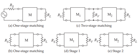
Figure \(\PageIndex{1}\): Matching in stages: (a) matching network \(\text{M}\) matching \(R_{S}\) to \(R_{L}\); (b) without an explicit source; (c) two-stage matching with a virtual resistor \(R_{V}\) ; (d) matching \(R_{S}\) to \(R_{V}\) ; and (e) matching \(R_{V}\) to \(R_{L}\).
to the load resistor \(R_{L}\). After \(M_{1}\) has been designed the resistance looking into the right-hand port of \(M_{1}\), see Figure \(\PageIndex{1}\)(d), will be \(R_{V}\) so \(R_{V}\) is the Thevenin equivalent source resistance to \(M_{2}\). Similarly the input impedance looking into the left-hand port of \(M_{2}\) is \(R_{V}\) so \(R_{V}\) is the effective load resistor of \(M_{1}\). Of course these are the impedances at the center frequency and away from the center frequency of the match the input impedances will be complex.
The concept behind multi-stage matching network design is shown in Figure \(\PageIndex{2}\) where the standard one-stage match is shown in Figure \(\PageIndex{2}\)(a). While this is shown for \(R_{L} > R_{S}\) the concept holds for \(R_{L} < R_{S}\). The arrows follow the convention that design begins with the load and ends at the source. With the one stage match the circuit \(Q\) is fixed designated here as the total circuit \(Q\), \(Q_{T}\) being the same as the \(Q\) of the one-stage \(R_{L}\) to \(R_{S}\) matching network, \(Q_{SL}\). The two-stage match that reduces bandwidth (compared to the one-stage match) is shown in Figure \(\PageIndex{2}\)(b). The total \(Q\), \(Q_{T}\), of the second stage is higher than for the one-stage design because the ratio of \(R_{L}\) to \(R_{V}\) is greater than the ratio of \(R_{V}\) to \(R_{S}\). Bandwidth can also be reduced relative to the one-stage match by assigning \(R_{V}\) to be greater than both \(R_{L}\) and \(R_{S}\), see Figure \(\PageIndex{2}\)(c).
Choosing \(R_{V}\) to be between \(R_{S}\) and \(R_{L}\) will result in a circuit with lower \(Q_{T}\) and the bandwidth of the match will increase, see Figure \(\PageIndex{2}\)(d). The maximum bandwidth for a two-stage match is to choose \(R_{V}\) as the geometric mean of \(R_{S}\) and \(R_{L}\). This concept can be extended to multiple stages as shown for a three-stage match in Figure \(\PageIndex{2}\)(e).
This section presents various matching network designs for manipulating bandwidth and all are based on the concept of choosing a virtual resistor.
6.6.2 Three-Element Matching Networks
With the L network (i.e., two-element matching), the circuit \(Q\) is fixed once the source and load resistances, \(R_{S}\) and \(R_{L}\), are fixed:
\[\label{eq:1}Q=\sqrt{\frac{R_{L}}{R_{S}}-1},\quad (R_{L}>R_{S}) \]
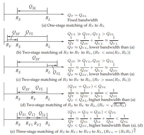
Figure \(\PageIndex{2}\): Effect of multi-stage matching on total circuit \(Q\), \(Q_{T}\), and matching bandwidth (which is approximately inversely proportional to \(Q_{T}\).)
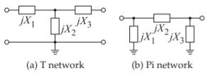
Figure \(\PageIndex{3}\): Two three-element matching networks.
Thus the designer does not have a choice of circuit \(Q\). Breaking the matching problem into parts enables the circuit \(Q\) to be controlled. Introducing a third element in the matching network provides the extra degree of freedom in the design for adjusting \(Q\), and hence bandwidth.
Two three-element matching networks, the \(\text{T}\) network and the Pi network, are shown in Figure \(\PageIndex{3}\). Which network is used depends on
- the realization constraints associated with the specific design, and
- the nature of the reactive parts of the source and load impedances and whether they can be used as part of the matching network.
The three-element matching network comprises \(2\) two-element (or \(\text{L}\)) matching networks and is used to increase the overall \(Q\) and thus narrow bandwidth. Given \(R_{S}\) and \(R_{L}\), the circuit \(Q\) established by an \(\text{L}\) matching network is the minimum circuit \(Q\) available in the three-element matching arrangement. With three-element matching, the \(Q\) can only increase, so three-element matching is used for narrowband (high-\(Q\)) applications. However, lower \(Q\) can be obtained with more than three elements. The next subsections consider matching with more than three elements.
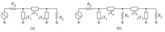
Figure \(\PageIndex{4}\): Pi matching networks: (a) view of a Pi network; and (b) as two back-to-back \(\text{L}\) networks with a virtual resistance, \(R_{V}\), between the networks.
6.6.3 The Pi Network
The Pi network may be thought of as two back-to-back \(\text{L}\) networks that are used to match the load and the source to a virtual resistance, \(R_{V}\), placed at the junction between the two networks, as shown in Figure \(\PageIndex{4}\)(b). The design of each section of the Pi network is as for the \(\text{L}\) network matching. \(R_{S}\) is matched to \(R_{V}\) and \(R_{V}\) is matched to \(R_{L}\).
\(R_{V}\) must be selected smaller than \(R_{S}\) and \(R_{L}\) since it is connected to the series arm of each \(\text{L}\) section. Furthermore, \(R_{V}\) can be any value that is smaller than the smaller of \(R_{S},\: R_{L}\). However, it is customarily used as the design parameter for specifying the desired \(Q\).
As a useful design approximation, the loaded \(Q\) of the Pi network can be taken as the \(Q\) of the \(\text{L}\) section with the highest \(Q\):
\[\label{eq:2}Q=\sqrt{\frac{\text{max}(R_{S},\:R_{L})}{R_{V}}-1} \]
Given \(R_{S},\: R_{L},\) and \(Q\), the above equation yields the value of \(R_{V}\).
Example \(\PageIndex{1}\): Three-Element Matching Network Design
Design a Pi network to match a \(50\:\Omega\) source to a \(500\:\Omega\) load. The desired \(Q\) is \(10\). A suitable matching network topology is shown in Figure \(\PageIndex{5}\) together with the virtual resistance, \(R_{V}\), to be used in design.
Solution
\(R_{S} = 50\:\Omega\) and \(R_{L} = 500\:\Omega\) so \(\text{max}(R_{S},\: R_{L}) = 500\:\Omega\) and so the virtual resistor is
\[\label{eq:3}R_{V}=\frac{\text{max}(R_{S},\:R_{L})}{Q^{2}+1}=\frac{500}{101}=4.95\:\Omega \]
Design proceeds by separately designing the \(\text{L}\) networks to the left and right of \(R_{V}\). For the \(\text{L}\) network on the left,
\[\label{eq:4}Q_{\text{left}}=\sqrt{\frac{50}{4.95}-1}=3.017,\quad\text{so}\quad Q_{\text{left}}=\frac{|X_{a}|}{R_{V}}=\frac{R_{S}}{|X_{1}|}=3.017 \]
Note that \(X_{1}\) and \(X_{a}\) must be of opposite types (one is capacitive and the other is inductive). The left \(\text{L}\) network has elements
\[\label{eq:5}|X_{a}|=14.933\:\Omega\quad\text{and}\quad |X_{1}|=16.6\:\Omega \]
For the \(\text{L}\) network on the right of \(R_{V}\),
\[\label{eq:6}Q_{\text{right}}=Q=10,\quad\text{thus}\quad\frac{|X_{b}|}{R_{V}}=\frac{R_{L}}{X_{3}}=10 \]
\(X_{b},\: X_{3}\) are of opposite types, and
\[\label{eq:7}|X_{b}|=49.5\:\Omega\quad\text{and}\quad |X_{3}|=50\:\Omega \]
The resulting Pi network is shown in Figure \(\PageIndex{6}\) with the values
\[\label{eq:8}|X_{1}|=16.6\:\Omega,\quad |X_{3}|=50\:\Omega,\quad |X_{a}|=14.933\:\Omega,\quad\text{and}\quad |X_{b}|=49.5\:\Omega \]
Note that the pair \(X_{a},\: X_{1}\) are of opposite types and similarly \(X_{b},\: X_{3}\) are of opposite types.
So there are four possible realizations, as shown in Figure \(\PageIndex{7}\).
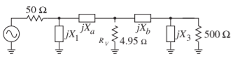
Figure \(\PageIndex{5}\): Matching network problem of Example \(\PageIndex{1}\).
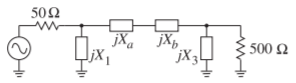
Figure \(\PageIndex{6}\): Final matching network in Example \(\PageIndex{1}\).
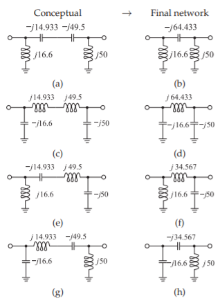
Figure \(\PageIndex{7}\): Four possible Pi matching networks: (a), (c), (e), and (g) conceptual circuits; and (b), (d), (f), and (h), respectively, their final reduced Pi networks.
In the previous example there were four possible realizations of the three-element matching network, and this is true in general. The specific choice of one of the four possible realizations will depend on specific application-related factors such as
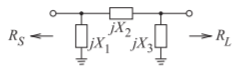
Figure \(\PageIndex{8}\): A three-element matching network.
- elimination of stray reactances,
- the need to pass or block DC current, and
- the need for harmonic filtering
It is fortunate that it may be possible to achieve multiple functions with the same network.
Example \(\PageIndex{2}\): Three-Element Matching with Reactive Source and Load
Design a Pi network to match the source to the load shown. The design frequency is \(900\text{ MHz}\) and the desired \(Q\) is \(10\).
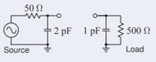
Figure \(\PageIndex{9}\)
Solution
The design objective is to arrive at an overall network which has a \(Q\) of \(10\). To achieve this it is necessary to absorb the source and load reactances into the matching network. If they were resonated instead, the overall \(Q\) of the network can be expected to higher than the \(Q\) of the \(\text{L}\) matching network on its own.
Design begins by considering the matching of \(R_{S} = 50\:\Omega\) to \(R_{L} = 500\:\Omega\). Since the \(Q\) is specified, three (or more) matching elements must be used. The design starting point is shown on the right:
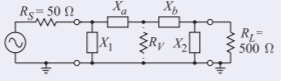
Figure \(\PageIndex{10}\)
The virtual resistor \(R_{V} = \text{max }(R_{s},\: R_{L})/(1 + Q_{2}) = (500\:\Omega)/(1 + 100) = 4.95\:\Omega\). The left subnetwork with \(X_{1}\) and \(X_{a}\) has \(Q_{\text{LEFT}} = \sqrt{R_{S}/R_{V} − 1} = \sqrt{50/4.95 − 1} = 3.017\). The right subnetwork with \(X_{2}\) and \(X_{b}\) has \(Q_{\text{RIGHT}} = \sqrt{R_{L}/R_{V} − 1} = \sqrt{500/4.95 − 1} = 10.001\).
Note that \(Q_{\text{RIGHT}}\) is almost exactly the desired \(Q\) of the network and \(Q_{\text{LEFT}}\) will have little effect on the \(Q\) of the overall circuit. Now \(Q_{\text{LEFT}} = |X_{a}|/R_{V} = R_{S}/|X_{1}|,\) so \(|X_{a}| = 14.9\:\Omega\) and \(|X_{1}| = 16.57\:\Omega\). \(Q_{\text{RIGHT}} = |X_{b}|/R_{V} = R_{S}/|X_{2}|,\) so \(|X_{b}| = 49.5\:\Omega\) and \(|X_{2}| = 50.0\:\Omega\).
\(X_{1}\) must be chosen to be a capacitor \(C_{1} = 10.67\text{ pF}\) so that the \(2\text{ pF}\) source capacitance can be absorbed. Similarly \(X_{2}\) is a capacitor \(C_{2} = 3.53\text{ pF}\). \(X_{a}\) and \(X_{b}\) are both inductors that combine in series for a total inductance \(L_{3} = 11.38\text{ nH}\). This leads to the final design shown on the right where the matching network is in the dashed box.
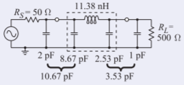
Figure \(\PageIndex{11}\)
6.6.4 Matching Network \(Q\) Revisited
To demonstrate that the circuit \(Q\) established by an \(\text{L}\) matching network is the minimum circuit \(Q\) for a network having at most three elements, consider the design equations for \(R_{S} > R_{L}\). Referring to Figure \(\PageIndex{8}\),
\[\label{eq:9}X_{1}=\frac{R_{S}}{Q},\quad X_{3}=R_{L}\left(\frac{R_{S}/R_{L}}{Q^{2}+1-R_{S}/R_{L}}\right)^{\frac{1}{2}},\quad X_{2}=\frac{QR_{S}+R_{S}R_{L}/X_{3}}{Q^{2}+1} \]
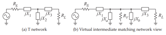
Figure \(\PageIndex{12}\): \(\text{T}\) network design approach.
Notice that the denominator of \(X_{3}\) can be written as
\[\label{eq:10}Q^{2}+1-\frac{R_{S}}{R_{L}}=\left(Q+\sqrt{\frac{R_{S}}{R_{L}}-1}\right)\left(Q-\sqrt{\frac{R_{S}}{R_{L}}-1}\right) \]
Then for a real solution we must have
\[\label{eq:11}Q\geq\sqrt{\frac{R_{S}}{R_{L}}-1} \]
and so \(Q\geq Q_{\text{L network}}\). For \(Q = Q_{\text{L network}},\: X_{3}\to ∞\) and the Pi network reduces to an \(\text{L}\) network that has two elements. Thus it is not possible to have a lower \(Q\) with a three-element matching network than the \(Q\) of a two-element matching network. Thus a three-element matching network must have lower bandwidth than that of a two-element matching network.
6.6.5 The \(\text{T}\) Network
The \(\text{T}\) network may be thought of as two back-to-back \(\text{L}\) networks that are used to match the load and the source to a virtual resistance, \(R_{V}\), placed at the junction between the two \(\text{L}\) networks (see Figure \(\PageIndex{12}\)). \(R_{V}\) must be selected to be larger than both \(R_{S}\) and \(R_{L}\) since it is connected to the shunt leg of each \(\text{L}\) section. \(R_{V}\) is chosen according to the equation
\[\label{eq:12}Q=\sqrt{\frac{R_{V}}{\text{min}(R_{S},\: R_{L})}-1} \]
where \(Q\) is the desired loaded \(Q\) of the network. Each \(\text{L}\) network is calculated in exactly the same manner as was done for the Pi network matching. That is, \(R_{S}\) is matched to \(R_{V}\) and \(R_{V}\) is matched to \(R_{L}\). Once again there will be four possible designs for the \(\text{T}\) network, given \(R_{S},\: R_{L},\) and \(Q\).
6.6.6 Broadband (Low \(Q\)) Matching
\(\text{L}\) network matching does not allow the circuit \(Q\), and hence bandwidth, to be selected. However, Pi network and \(\text{T}\) network matching allows the circuit \(Q\) to be selected independent of the source and load impedances, provided that the chosen \(Q\) is larger than that which can be obtained with an \(\text{L}\) network. Thus the Pi and \(\text{T}\) networks result in narrower bandwidth designs.
One design solution for broadband matching is to use two (or more) series-connected \(\text{L}\) sections (see Figure \(\PageIndex{13}\)). Design is still based on the concept of a virtual resistor, \(R_{V}\), placed at the junction of the two \(\text{L}\) networks (as in Figure \(\PageIndex{14}\)), but now \(R_{V}\) is chosen to be between \(R_{S}\) and \(R_{L}\):
\[\label{eq:13}R_{\text{min}}\leq R_{V}\leq R_{\text{max}} \]
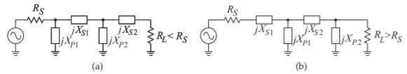
Figure \(\PageIndex{13}\): Broadband matching networks.
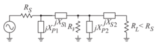
Figure \(\PageIndex{14}\): Matching network with two \(\text{L}\) networks.
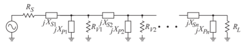
Figure \(\PageIndex{15}\): Cascaded \(\text{L}\) networks for broadband matching.
where \(R_{\text{min}} = \text{min}(R_{L},\: R_{S})\) and \(R_{\text{max}} = \text{max}(R_{L},\: R_{S})\). Then one of the two networks will have
\[\label{eq:14}Q_{1}=\sqrt{\frac{R_{V}}{R_{\text{min}}}-1}\quad\text{and the other}\quad Q_{2}=\sqrt{\frac{R_{\text{max}}}{R_{V}}-1} \]
The maximum bandwidth (minimum \(Q\)) available is obtained when
\[\label{eq:15}Q_{1}=Q_{2}=\sqrt{\frac{R_{V}}{R_{\text{min}}}-1}=\sqrt{\frac{R_{\text{max}}}{R_{V}}-1} \]
That is, the maximum matching bandwidth is obtained when \(R_{V}\) is the geometric mean of \(R_{S}\) and \(R_{L}\):
\[\label{eq:16}R_{V}=\sqrt{R_{L}R_{S}} \]
Even wider bandwidths can be obtained by cascading more than two \(\text{L}\) networks, as shown in Figure \(\PageIndex{15}\). In this circuit
\[\label{eq:17}R_{S}<R_{V1}<R_{V2}\ldots R_{V_{n}-1}<R_{L} \]
For optimum bandwidth the ratios should be equal,
\[\label{eq:18}\frac{R_{V_{1}}}{R_{S}}=\frac{R_{V_{2}}}{R_{V_{1}}}=\frac{R_{V_{3}}}{R_{V_{2}}}=\cdots=\frac{R_{L}}{R_{V_{n}-1}} \]
and the \(Q\) is given by
\[\label{eq:19}Q=\sqrt{\frac{R_{V_{1}}}{R_{S}}-1}=\sqrt{\frac{R_{V_{2}}}{R_{1}}-1}=\cdots=\sqrt{\frac{R_{L}}{R_{V_{n}-1}}-1} \]
If there are \(N\) \(\text{L}\) networks used in the match, the maximum bandwidth will be obtained if the \(i\)th virtual resistor is
\[\label{eq:20}R_{Vi}=(R_{S}R_{L})^{i/N},\quad i=1,\ldots,(N-1) \]
Example \(\PageIndex{3}\): Two-Section Matching Network Design
Consider matching a \(10\:\Omega\) source to a \(1000\:\Omega\) load using two \(\text{L}\) matching networks and designing for a \(Q\) of \(3\). How many matching sections are required?
Solution
Here the approximate \(Q\)s achieved with a single \(\text{L}\) matching network and with an optimum two-section design are compared. For a single \(\text{L}\) network design
\[\label{eq:21}Q=\sqrt{\frac{R_{L}}{R_{S}}-1}=9.95 \]
Now consider an optimum two-section design:
\[\label{eq:22}R_{V}=\sqrt{R_{S}R_{L}};\quad Q_{2}=\sqrt{\frac{R_{L}}{R_{V}}-1}=\sqrt{\sqrt{\frac{R_{L}}{R_{S}}}-1}=3 \]
Thus the \(Q\) is \(3\) compared to the \(Q\) of an \(\text{L}\) section of \(9.95\). If the fractional bandwidth is inversely proportional to \(Q\), then the bandwidth of the two-section design is \(9.95/3 = 3.32\) times more than that of the \(\text{L}\) section.
Now consider how many sections are required to obtain a \(Q\) of \(2\):
\[\begin{align}\label{eq:23}(1+Q^{2})&=\frac{R_{V_{1}}}{R_{S}}=\frac{R_{V_{2}}}{R_{V_{1}}}=\ldots=\frac{R_{L}}{R_{V_{n}-1}}\Rightarrow \\ \label{eq:24} (1+Q^{2})^{n}&=\frac{R_{L}}{R_{S}}\Rightarrow n\ln (1+Q^{2})=\ln\frac{R_{L}}{R_{S}}\Rightarrow n=\frac{\ln (R_{L}/R_{S})}{\ln (1+Q^{2})}\end{align} \]
For \(Q = 2\) and \(R_{L}/R_{S} = 100\), \(n = 2.86\), which rounds to \(n = 3\), and three sections are required.