
2.6: Reflections at Interfaces
- Page ID
- 41017

\( \newcommand{\vecs}[1]{\overset { \scriptstyle \rightharpoonup} {\mathbf{#1}} } \)
\( \newcommand{\vecd}[1]{\overset{-\!-\!\rightharpoonup}{\vphantom{a}\smash {#1}}} \)
\( \newcommand{\id}{\mathrm{id}}\) \( \newcommand{\Span}{\mathrm{span}}\)
( \newcommand{\kernel}{\mathrm{null}\,}\) \( \newcommand{\range}{\mathrm{range}\,}\)
\( \newcommand{\RealPart}{\mathrm{Re}}\) \( \newcommand{\ImaginaryPart}{\mathrm{Im}}\)
\( \newcommand{\Argument}{\mathrm{Arg}}\) \( \newcommand{\norm}[1]{\| #1 \|}\)
\( \newcommand{\inner}[2]{\langle #1, #2 \rangle}\)
\( \newcommand{\Span}{\mathrm{span}}\)
\( \newcommand{\id}{\mathrm{id}}\)
\( \newcommand{\Span}{\mathrm{span}}\)
\( \newcommand{\kernel}{\mathrm{null}\,}\)
\( \newcommand{\range}{\mathrm{range}\,}\)
\( \newcommand{\RealPart}{\mathrm{Re}}\)
\( \newcommand{\ImaginaryPart}{\mathrm{Im}}\)
\( \newcommand{\Argument}{\mathrm{Arg}}\)
\( \newcommand{\norm}[1]{\| #1 \|}\)
\( \newcommand{\inner}[2]{\langle #1, #2 \rangle}\)
\( \newcommand{\Span}{\mathrm{span}}\) \( \newcommand{\AA}{\unicode[.8,0]{x212B}}\)
\( \newcommand{\vectorA}[1]{\vec{#1}} % arrow\)
\( \newcommand{\vectorAt}[1]{\vec{\text{#1}}} % arrow\)
\( \newcommand{\vectorB}[1]{\overset { \scriptstyle \rightharpoonup} {\mathbf{#1}} } \)
\( \newcommand{\vectorC}[1]{\textbf{#1}} \)
\( \newcommand{\vectorD}[1]{\overrightarrow{#1}} \)
\( \newcommand{\vectorDt}[1]{\overrightarrow{\text{#1}}} \)
\( \newcommand{\vectE}[1]{\overset{-\!-\!\rightharpoonup}{\vphantom{a}\smash{\mathbf {#1}}}} \)
\( \newcommand{\vecs}[1]{\overset { \scriptstyle \rightharpoonup} {\mathbf{#1}} } \)
\( \newcommand{\vecd}[1]{\overset{-\!-\!\rightharpoonup}{\vphantom{a}\smash {#1}}} \)
\(\newcommand{\avec}{\mathbf a}\) \(\newcommand{\bvec}{\mathbf b}\) \(\newcommand{\cvec}{\mathbf c}\) \(\newcommand{\dvec}{\mathbf d}\) \(\newcommand{\dtil}{\widetilde{\mathbf d}}\) \(\newcommand{\evec}{\mathbf e}\) \(\newcommand{\fvec}{\mathbf f}\) \(\newcommand{\nvec}{\mathbf n}\) \(\newcommand{\pvec}{\mathbf p}\) \(\newcommand{\qvec}{\mathbf q}\) \(\newcommand{\svec}{\mathbf s}\) \(\newcommand{\tvec}{\mathbf t}\) \(\newcommand{\uvec}{\mathbf u}\) \(\newcommand{\vvec}{\mathbf v}\) \(\newcommand{\wvec}{\mathbf w}\) \(\newcommand{\xvec}{\mathbf x}\) \(\newcommand{\yvec}{\mathbf y}\) \(\newcommand{\zvec}{\mathbf z}\) \(\newcommand{\rvec}{\mathbf r}\) \(\newcommand{\mvec}{\mathbf m}\) \(\newcommand{\zerovec}{\mathbf 0}\) \(\newcommand{\onevec}{\mathbf 1}\) \(\newcommand{\real}{\mathbb R}\) \(\newcommand{\twovec}[2]{\left[\begin{array}{r}#1 \\ #2 \end{array}\right]}\) \(\newcommand{\ctwovec}[2]{\left[\begin{array}{c}#1 \\ #2 \end{array}\right]}\) \(\newcommand{\threevec}[3]{\left[\begin{array}{r}#1 \\ #2 \\ #3 \end{array}\right]}\) \(\newcommand{\cthreevec}[3]{\left[\begin{array}{c}#1 \\ #2 \\ #3 \end{array}\right]}\) \(\newcommand{\fourvec}[4]{\left[\begin{array}{r}#1 \\ #2 \\ #3 \\ #4 \end{array}\right]}\) \(\newcommand{\cfourvec}[4]{\left[\begin{array}{c}#1 \\ #2 \\ #3 \\ #4 \end{array}\right]}\) \(\newcommand{\fivevec}[5]{\left[\begin{array}{r}#1 \\ #2 \\ #3 \\ #4 \\ #5 \\ \end{array}\right]}\) \(\newcommand{\cfivevec}[5]{\left[\begin{array}{c}#1 \\ #2 \\ #3 \\ #4 \\ #5 \\ \end{array}\right]}\) \(\newcommand{\mattwo}[4]{\left[\begin{array}{rr}#1 \amp #2 \\ #3 \amp #4 \\ \end{array}\right]}\) \(\newcommand{\laspan}[1]{\text{Span}\{#1\}}\) \(\newcommand{\bcal}{\cal B}\) \(\newcommand{\ccal}{\cal C}\) \(\newcommand{\scal}{\cal S}\) \(\newcommand{\wcal}{\cal W}\) \(\newcommand{\ecal}{\cal E}\) \(\newcommand{\coords}[2]{\left\{#1\right\}_{#2}}\) \(\newcommand{\gray}[1]{\color{gray}{#1}}\) \(\newcommand{\lgray}[1]{\color{lightgray}{#1}}\) \(\newcommand{\rank}{\operatorname{rank}}\) \(\newcommand{\row}{\text{Row}}\) \(\newcommand{\col}{\text{Col}}\) \(\renewcommand{\row}{\text{Row}}\) \(\newcommand{\nul}{\text{Nul}}\) \(\newcommand{\var}{\text{Var}}\) \(\newcommand{\corr}{\text{corr}}\) \(\newcommand{\len}[1]{\left|#1\right|}\) \(\newcommand{\bbar}{\overline{\bvec}}\) \(\newcommand{\bhat}{\widehat{\bvec}}\) \(\newcommand{\bperp}{\bvec^\perp}\) \(\newcommand{\xhat}{\widehat{\xvec}}\) \(\newcommand{\vhat}{\widehat{\vvec}}\) \(\newcommand{\uhat}{\widehat{\uvec}}\) \(\newcommand{\what}{\widehat{\wvec}}\) \(\newcommand{\Sighat}{\widehat{\Sigma}}\) \(\newcommand{\lt}{<}\) \(\newcommand{\gt}{>}\) \(\newcommand{\amp}{&}\) \(\definecolor{fillinmathshade}{gray}{0.9}\)Transmission lines transfer power from one point to another and there are often many interfaces at which power is reflected and transferred. This section is focused on developing an intuitive understanding of reflection and transmission of power at interfaces and over a transmission line. Section 2.6.1 presents an understanding of power flow and introduces the return loss concept applying this analysis to a single interface in Section 2.6.3. Microwave engineering is greatly concerned with maximum power transfer and the analysis that supports design choices, the maximum power transfer theorem, is revisited in Section 2.6.2. Section 2.6.4 presents bounce diagram analysis which is concerned with reflection and transmission at multiple interfaces. This can be a confusing analysis but it provides the essential understanding for the development of intuition for how power flows, and understanding of situations where power flow may be disrupted. The final section, Section 2.6.5, presents the theory of small reflections, derived from bounce diagram analysis, which is used in several places in this book series in the synthesis of transmission line networks.
2.6.1 Power Flow and Return Loss
Now consider the power flow on the lossless line in Figure 2.3.1. The incident (forward-traveling) wave has the power
\[\begin{align}P^{+}&=\frac{1}{2}\Re\left[V^{+}(I^{+})^{\ast}\right]=\frac{1}{2}\Re\left[V^{+}\left(\frac{V^{+}}{Z_{0}}\right)^{\ast}\right]\nonumber \\ \label{eq:1}&=\frac{1}{2}\Re\left\{(V_{0}^{+}e^{-\jmath\beta z})\left(\frac{V_{0}^{+}e^{-\jmath\beta z}}{Z_{0}}\right)^{\ast}\right\}=\frac{1}{2}\frac{|V_{0}^{+}|^{2}}{Z_{0}}\end{align} \]
and the reflected wave has the power (using Equation (2.3.7))
\[\label{eq:2}P^{-}=\frac{1}{2}\frac{|V_{0}^{-}|^{2}}{Z_{0}}=\frac{|\Gamma|^{2}}{2}\frac{|V_{0}^{+}|^{2}}{Z_{0}} \]
Considering conservation of power, the power delivered to the load, \(P_{L}\), is the difference of the forward- and backward-traveling powers:
\[\label{eq:3}P_{L}=\frac{1}{2}\Re\{V_{L}I_{L}^{\ast}\}=P^{+}-P^{-}=P^{+}\left(1-|\Gamma|^{2}\right) \]
Noteworthy cases are when there is an open circuit, a short circuit, or a purely reactive load at the end of a transmission line. These have \(|\Gamma| = 1\). Thus all power is reflected back to the source and \(P_{L} = 0\).
The power that is absorbed by the load appears as a loss as far as the incident and reflected waves are concerned. To describe this, the concept of return loss (RL) is introduced and defined as
\[\label{eq:4}\text{RL}=-20\log|\Gamma|\text{ dB} \]
RL indicates the available power not delivered to the load. A matched load \((\Gamma=0)\) has \(\text{RL} =\infty\text{ dB}\), and a total reflection \((|\Gamma| = 1)\) has \(\text{RL} = 0\text{ dB}\).
A transmission line with a characteristic impedance of \(75\:\Omega\) supports a forward-traveling wave with a power of \(1\:\mu\text{W}\). The line is terminated in a resistance of \(100\:\Omega\). Draw the lumped-element equivalent circuit at the interface between the transmission line and the load.
Solution
The equivalent circuit has the form
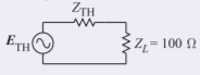
Figure \(\PageIndex{1}\)
where \(E_{\text{TH}}\) is the Thevenin equivalent generator and \(Z_{\text{TH}}\) is the Thevenin equivalent generator impedance.
The amplitude of the forward-traveling voltage wave is obtained by calculating the power in the forward-traveling wave:
\[P^{+}=\frac{1}{2}(V^{+})^{2}/Z_{0}=(V^{+})^{2}/150=1\:\mu\text{W}=10^{-6}\text{ W}\nonumber \]
So \(V^{+} =\sqrt{150\cdot 10^{−6}} = 12.25\text{ mV}\). Note that \(V^{+}\) is not \(E_{\text{TH}}\). To calculate \(E_{\text{TH}}\), consider the circuit to the right that results in maximum power transfer.
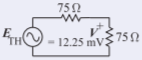
Figure \(\PageIndex{2}\)
So \(E_{\text{TH}} = 2V^{+} = 24.5\text{ mV}\). Since the line has a characteristic impedance of \(75\:\Omega\), then \(Z_{\text{TH}} = 75\:\Omega\). So the lumped-element equivalent circuit at the load is
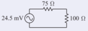
Figure \(\PageIndex{3}\)
2.6.2 Maximum Power Transfer Theorem
Many transmission line calculations can be solved using the concepts of maximum available power, incident power, and reflected power. At microwave frequencies the output impedance of sources, for example, cannot be ignored as can often be done at low frequencies. Thus the output of an RF source is defined in terms of maximum available power.
Consider the source shown in Figure \(\PageIndex{4}\) with an impedance \(Z_{S} = R_{S} +\jmath X_{S}\) driving a load \(Z_{L} = R_{L} +\jmath X_{L}\). The aim here is to find \(Z_{L}\) for maximum delivery of power to the load. The phasor current in the load is
\[\label{eq:5}I=\frac{E}{Z_{S}+Z_{L}} \]
and thus the average power in the load is
\[\label{eq:6}P_{L}=\frac{1}{2}|I|^{2}R_{L}=\frac{1}{2}\left(\frac{|E|}{|Z_{S}+Z_{L}|}\right)^{2}R_{L}=\frac{\frac{1}{2}|E|^{2}R_{L}}{(R_{S}+R_{L})^{2}+(X_{S}+X_{L})^{2}} \]
The load required for maximum power transfer is obtained by first considering a fixed value of \(R_{L}\) and then finding the value of \(X_{L}\) required to minimize
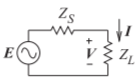
Figure \(\PageIndex{4}\): A source terminated in a load. Maximum power transfer occurs when \(Z_{L} = Z_{S}^{\ast}\).
Equation \(\eqref{eq:6}\). Since \(X_{L}\) only affects the denominator in Equation \(\eqref{eq:6}\), it is clear that the denominator is minimized by making \(X_{L} = −X_{S}\). So now Equation \(\eqref{eq:6}\) reduces to
\[\label{eq:7}P_{L}=\frac{\frac{1}{2}|E|^{2}R_{L}}{(R_{S}+R_{L})^{2}} \]
and
\[\label{eq:8}P_{L}=\frac{\frac{1}{2}|E|^{2}}{(R_{S}^{2}/R_{L}+2R_{S}+R_{L})} \]
Now the power delivered to the load is maximized by minimizing the denominator in Equation \(\eqref{eq:8}\), which will occur when the derivative of the denominator in Equation \(\eqref{eq:8}\) is zero. That is, when
\[\label{eq:9}\frac{d}{dR_{L}}(R_{S}^{2}/R_{L}+2R_{S}+R_{L})^{2}=\frac{-R_{S}^{2}}{R_{L}^{2}}+1=0 \]
The derivative is zero when
\[\label{eq:10}R_{S}^{2}/R_{L}^{2}=1,\quad\text{that is, when}\quad R_{L}=\pm R_{S} \]
When the derivative is zero, the power transferred to the load is either the minimum or maximum power that can be delivered to the load. Clearly \(R_{L} = −R_{S}\) is a nonsensical solution as the load and source resistance should be positive. In addition, the situations at the extremes need to be check, that is, when \(R_{L}\) is very small, \(R_{L}\to 0\), and when \(R_{L}\) is very large, \(R_{L}\to\infty\). As \(R_{L}\to 0\), Equation \(\eqref{eq:7}\) becomes \(P_{L}\to 0\), and as \(R_{L}\to\infty\), Equation \(\eqref{eq:7}\) becomes \(P_{L}\to 0\). Clearly there will not be negative power dissipated in \(R_{L}\), so when \(R_{L} = R_{S}\) the maximum power, \(P_{L}|_{\text{max}}\), is dissipated in the load. Equation \(\eqref{eq:7}\) becomes
\[\label{eq:11}P_{L}|_{\text{max}}=\frac{1}{2}\frac{|E|^{2}R_{L}}{(R_{S}+R_{S})^{2}}=\frac{1}{8}\frac{|E|^{2}}{R_{S}} \]
This is called the maximum available power, or simply the available power of the source. So the conditions for maximum power transfer are \(R_{L} = R_{S}\) and \(X_{L} = −X_{S}\); that is, the maximum power transfer from source to load requires
\[\label{eq:12}Z_{L}=Z_{S}^{\ast} \]
Also note that if the source impedance in Figure \(\PageIndex{4}\) is resistive, \(V =\frac{1}{2}E\) at maximum power transfer.
A \(75\:\Omega\) source with an available power of \(1\text{ W}\) is terminated in a short circuit. What is the power dissipated in the Thevenin equivalent resistance of the source?
Solution
At RF, “\(75\:\Omega\) source” refers to a source with a Thevenin equivalent resistance of \(75\:\Omega\) which here is \(Z_{S}\). The condition for maximum power transfer, and when the full available power is delivered to the load, is when the load impedance, \(Z_{L}\) is the complex conjugate of \(Z_{S} = 75\:\Omega\). The circuit for maximum power transfer is as shown to the right.
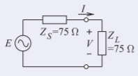
Figure \(\PageIndex{5}\)
To solve the problem we must determine \(E\) as this will not change even though the current through \(Z_{S}\), \(I\), will depend on the load impedance. The available power is
\[P_{A} = \frac{1}{2}|I|^{2}\Re(Z_{S}) = \frac{1}{2}|I|^{2}\times 75 = 1\text{ W}\text{ and so }I =\sqrt{2\times 1/75} = 0.1633\text{ A}\nonumber \]
From this the voltage across the load can be determine:
\[V = IZ_{L} = 0.1633\times 75 = 12.25\text{ V}\text{ and from symmetry }E = 2V = 24.50\text{ V}\nonumber \]
Now the condition with a short circuit, \(Z_{L} = 0\), can be determined. Note that \(I\) and \(V\) will change but \(E\) will be fixed.
Considering the circuit to the right, now
\[I = E/(Z_{S} + Z_{L}) = 24.50/(75 + 0) = 0.3267\text{ A}\nonumber \]
The power dissipated in \(Z_{S}\) is
\[P_{S} =\frac{1}{2}I^{2}\Re(Z_{S}) = 0.3267\times 75 = 4.002\text{ W}\nonumber \]
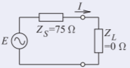
Figure \(\PageIndex{6}\)
Some comments on this result can be made. With a short circuit the current that flows in the circuit doubles compared to the maximum power transfer condition. Since the power dissipated in \(Z_{S}\) is proportion to the square of the current the power dissipated in the Thevenin equivalent resistance increases by a factor of \(4\) (\(P_{S}\) should be exactly \(4\text{ W}\)). The ideal voltage source \(E\) can provide unlimited power. However no matter what the value of \(Z_{L}\), the power dissipated in \(Z_{L}\) can never be more than the available power.
A transmission line is driven by a generator with a maximum available power of \(20\text{ dBm}\) and a Thevenin equivalent impedance of \(50\:\Omega\). The transmission line has a characteristic impedance of \(50\:\Omega\).
- What is the Thevenin equivalent generator voltage?
- What is the magnitude of the forward-traveling voltage wave on the line? Assume that the line is infinitely long.
- What is the power of the forward-traveling voltage wave?
Solution
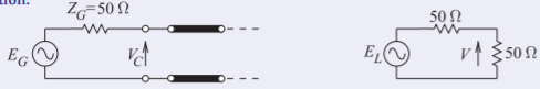
Figure \(\PageIndex{7}\)
- Maximum available power is delivered to the load when it is conjugately matched to the generator impedance (see right diagram). Then \(P_{\text{LOAD}} =\frac{1}{2}V^{2}/R\) (\(V\) is peak voltage) (i.e., \(P_{\text{LOAD}} = 20\text{ dBm} = 0.1\text{ W}\)) and
\[V=\sqrt{2P_{\text{LOAD}}\cdot R}=\sqrt{2\times 0.1\times 50}\text{ V}_{\text{peak}}=3.16\text{ V,}\quad E_{G}=2V=6.32\text{ V}\nonumber \] - This is just \(V\), so \(V^{+}= 3.16\text{ V}\).
- \(P^{+} = 20\text{ dBm}\).
2.6.3 A Single Interface
Many transmission line calculations are most conveniently addressed using the maximum available power concept. This is particularly so when there are multiple transmission lines. The concept is that the maximum available power from a source is incident on a load and if there is a mismatch, power is reflected and the rest of the power is transmitted. The circuits used to illustrate these calculations are shown in Figure \(\PageIndex{8}\). The available power of the source is \(P_{\text{av}}\), which is incident on the reference plane shown in Figure \(\PageIndex{8}\)(b) where it is called the incident power \(P_{I}\). At the reference plane power
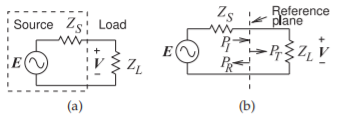
Figure \(\PageIndex{8}\): Calculations using incident and reflected power: (a) source terminated in a load; and (b) reference plane illustrating the use of incident and reflected power at a load.
is reflected, \(P_{R}\), and power is transmitted, \(P_{T}\). Using the reflection coefficient normalized to the impedance of the source (i.e., \(Z_{S}\))
\[\label{eq:13}P_{R}=|\Gamma|^{2}P_{I} \]
where
\[\label{eq:14}\Gamma=\frac{Z_{S}-Z_{L}}{Z_{S}+Z_{L}} \]
and the transmitted power is
\[\label{eq:15}P_{T}=\left(1-|\Gamma|^{2}\right)P_{I} \]
The transmission line shown in Figure 2.5.1(b) consists of a source with Thevenin impedance \(Z_{1} = 40\:\Omega\) and source \(E = 5\text{ V}\) (peak), connected to a \(\lambda /4\) long line of characteristic impedance \(Z_{01} = 40\:\Omega\), which in turn is connected to an infinitely long line of characteristic impedance \(Z_{02} = 100\:\Omega\). The transmission lines are lossless. Two reference planes are shown in Figure 2.5.1(b). At reference plane \(\mathsf{1}\) the incident power is \(P_{I1}\) (the maximum available power from the source), the reflected power is \(P_{R1}\), and the transmitted power is \(P_{T1}\). \(P_{I2}\) (the maximum available power from \(Z_{01}\)), \(P_{R2}\), and \(P_{T2}\) are similar quantities at Reference Plane \(\mathsf{2}\). \(P_{I1},\: P_{R1},\: P_{T1},\: P_{I2},\: P_{R2},\) and \(P_{T2}\) are steady-state quantities.
- What is \(P_{I1}\)?
- What is \(P_{T2}\)?
Solution
Since the infinitely long line does not have a backward-traveling wave this problem reduces to a single transmission line interface problem.
First develop some expectations. This will be a sanity check during the problem. \(P_{I1}\) and \(P_{I2}\) are maximum available powers and since the \(Z_{01}\) line (this is a short way of talking about the line with a characteristic impedance \(Z_{01}\)) is lossless they should be equal: \(P_{I1} = P_{I2}\). \(P_{T1}\) and \(P_{T2}\) are the total powers delivered to the right of the respective interfaces. Again since the \(Z_{01}\) line is lossless \(P_{T1} = P_{T2}\), Also \(P_{T1} ≤ P_{I1}\) as power \(P_{R1}\) is reflected from the interface. Similarly \(P_{T2} ≤ P_{I2}\).
- \(P_{I1}\) is the available power from the generator. Since the Thevenin impedance of the generator is \(40\:\Omega\), \(P_{I1}\) is the power that would be delivered to a matched load (the maximum available power). An equivalent problem is shown to the right where \(V =\frac{1}{2}E = 2.5 \text{ V}_{\text{peak}}\). So
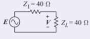
Figure \(\PageIndex{9}\)
\[\label{eq:16}P_{I1}=\text{ power in }Z_{L}=\frac{1}{2}(V)^{2}\frac{1}{Z_{L}}=\frac{1}{2}(2.5)^{2}\frac{1}{40}=0.07813\text{ W}=78.13\text{ mW} \]
Note that the \(\frac{1}{2}\) occurs because peak voltage is used in RF calculations. - Now the problem becomes interesting and there are many ways to solve it. One of the key observations is that the first transmission line has the same characteristic impedance as the Thevenin equivalent impedance of the generator, \(Z_{01} = Z_{1}\), and so can be ignored where appropriate. This observation will be used in this example. One way to proceed is to directly calculate \(P_{T2}\), and a second approach is to calculate the incident and reflected powers at reference plane \(\mathsf{2}\) and then to determine \(P_{T2}\).
- First approach: looking to the left from reference plane \(\mathsf{2}\), the circuit can be modeled as an equivalent circuit having a Thevenin equivalent resistance of \(40\:\Omega\) and a Thevenin equivalent voltage that has an available power of \(78.13\text{ mW}\). So in the circuit to the right, \(E_{2}\) is just \(E\) or \(5\text{ V}\).
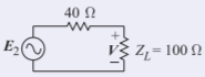
Figure \(\PageIndex{10}\)
The load is \(100\:\Omega\) as the second transmission line is infinitely long. A reasonable question to ask is why \(E_{2}\) is not \(2.5\text{ V}\), as this would be the voltage across \(Z_{L} = 40\:\Omega\) in part (a). However, \(2.5\text{ V}\) is the voltage of the forward-traveling voltage wave on the first transmission line with characteristic impedance \(Z_{01} = 40\:\Omega\). It is not the Thevenin equivalent voltage of the source. The voltage across the load is
\[\label{eq:17}V=E_{2}\frac{100}{40+100}=E\frac{100}{140}=3.57\text{ V}_{\text{peak}} \]
The power transmitted at reference plane \(\mathsf{2}\) is also the power delivered to the load:
\[\label{eq:18}P_{T2}=P_{L}=\frac{1}{2}(V)^{2}\frac{1}{Z_{L}}=\frac{1}{2}(3.57)^{2}\frac{1}{100}=0.0638\text{ W}=63.8\text{ mW} \]
A quick check is that this is less than \(P_{I1}\), as it should be. - Second approach: This time \(P_{R2}\), the reflected power at reference plane \(\mathsf{2}\), will be calculated. The incident power at plane \(\mathsf{2}\), \(P_{I2}\), is just \(P_{I1}\). \(P_{I2}\) is the maximum available power at reference plane \(\mathsf{2}\) and not necessarily the power that is incident there. In general, to calculate \(P_{I2}\) the Thevenin equivalent source looking to the left from reference plane \(\mathsf{2}\) would need to be calculated. However since here \(Z_{01} = Z_{1},\: P_{I2} = P_{I1} = 78.13\text{ mW}\).
\(P_{R2}\) can be calculated from the voltage reflection coefficient at reference plane \(\mathsf{2}\):
\[\begin{align}\label{eq:19}\Gamma_{2}&=\frac{Z_{L}-Z_{01}}{Z_{L}+Z_{01}}=\frac{100-40}{100+40}=0.429 \\ \label{eq:20}P_{R2}&=\Gamma_{2}^{2}P_{12}=0.429^{2}\times 78\text{ mW}=14.36\text{ mW}\end{align} \]
So \(P_{T2} = P_{I2} − P_{R2} = 78.13\text{ mW} − 14.36\text{ mW} = 63.7\text{ mW}\), which is the same as the transmitted power calculated in the first approach, allowing for rounding error. - A third approach is to calculate the input impedance looking to the right from reference plane \(\mathsf{1}\), call this \(Z_{\text{in}1}\). Using the lossless telegrapher’s equation, Equation 2.3.18, \(Z_{\text{in}1}\) is calculated to be \(16\:\Omega\).
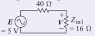
Figure \(\PageIndex{11}\)
The voltage across the \(16\:\Omega\) resistor is \(16/(40 + 16)(5\text{ V}) = 1.429\text{ V}\). So the power dissipated in \(Z_{\text{in}1}\) is
\[P=\frac{1}{2}(1.429\text{ V})^{2}\frac{1}{16}=0.0638\text{ W}=63.8\text{ mW}\nonumber \]
as before. All of this power must be transmitted to the infinitely long line, i.e. it is \(P_{T2}\), as the system is otherwise lossless.
- First approach: looking to the left from reference plane \(\mathsf{2}\), the circuit can be modeled as an equivalent circuit having a Thevenin equivalent resistance of \(40\:\Omega\) and a Thevenin equivalent voltage that has an available power of \(78.13\text{ mW}\). So in the circuit to the right, \(E_{2}\) is just \(E\) or \(5\text{ V}\).
2.6.4 Bounce Diagram
A bounce diagram is a graphical representation of reflections at the interfaces between networks. A microwave network is shown in Figure \(\PageIndex{12}\) where there are two reference planes at boundaries between different parts of the network. At each boundary there are reflections and transmissions of what could be viewed as small packets of sinusoidal signals. While the bounce diagram yields a steady-state result such as the input impedance, the thought experiment is that small sinusoidal packets bounce around the transmission-line network. Bounce diagrams are used to explore the impact of multiple reflections in a network leading to understanding, and from that to design decisions. Bounce diagrams are best illustrated through an example.
Reflection and Transmission Coefficients at a Boundary
Bounce diagram analysis requires that the reflection and transmission coefficients at a boundary be referenced to a common impedance. Figure \(\PageIndex{13}\)(a) shows the interface of two transmission lines of characteristic impedance \(Z_{01}\) and \(Z_{02}\) at a reference plane. The problem is determining the reflection coefficient, \(\Gamma\), and transmission coefficient, \(T\), at the boundary referencing them to the same impedance. Here they will be referenced to \(Z_{01}\). The reflection coefficient as seen from the \(Z_{01}\) line referenced to \(Z_{01}\) is
\[\label{eq:21}\Gamma=\frac{Z_{02}-Z_{01}}{Z_{02}+Z_{01}} \]
Now the transmission coefficient referenced to \(Z_{01}\) is
\[\label{eq:22}T=^{Z01}V_{2}^{+}/V_{1}^{+} \]
where \(^{Z01}V_{2}^{+}\) is the forward-traveling voltage wave on the \(Z_{02}\) line (traveling to the right) referenced to \(Z_{01}\). It is not the actual forward-traveling voltage on the \(Z_{02}\) line. \(V_{1}^{+} = ^{Z01}V_{1}^{+}\) is the traveling voltage wave on the \(Z_{01}\) line that is incident at the boundary. It is obtained using the circuit in Figure \(\PageIndex{13}\)(b). Figure \(\PageIndex{13}\)(b) shows the maximum power transfer condition so that
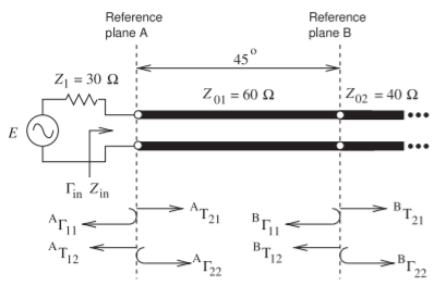
Figure \(\PageIndex{12}\): Transmission line network with a finite-length line of characteristic impedance \(Z_{01}\) and an infinitely long transmission line of characteristic impedance \(Z_{02}\). \(^{A}\Gamma_{1i}\) is the \(i\)th discrete reflection of an incident wave at the left-hand side of reference plane \(\mathsf{A}\). \(^{A}T_{1i}\) is the transmission at reference plane \(\mathsf{A}\) for the same event. \(^{A}\Gamma_{2i}\) is the \(i\)th discrete reflection of an incident wave at the right-hand side of reference plane \(\mathsf{A}\).
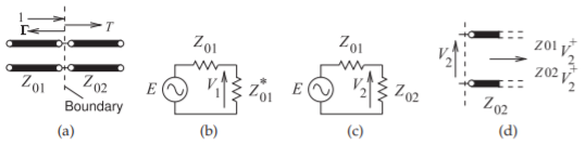
Figure \(\PageIndex{13}\): Reflection (\(\Gamma\)) and transmission (\(T\)) at the boundary between two transmission lines of characteristic impedance \(Z_{01}\) and \(Z_{02}\).
the forward-traveling wave on the \(Z_{01}\) line at the left of the boundary is
\[\label{eq:23}V_{1}^{+}=V_{1}=E\frac{Z_{01}}{Z_{01}+Z_{01}^{\ast}}=E\frac{Z_{01}}{2\Re(Z_{01})} \]
(For real impedances \(V_{1}^{+} =\frac{1}{2}E\).)
The next parameter to determine is \(^{Z01}V_{2}^{+}\). This begins by determining the total voltage, \(V_{2}\), at the boundary using the circuit in Figure \(\PageIndex{13}\)(c):
\[\label{eq:24}V_{2}=E\frac{Z_{02}}{Z_{01}+Z_{02}} \]
Now consider that the \(Z_{02}\) line is infinitely long, then it is clear that \(V_{2} = ^{Z02}V_{2}^{+}\). This is the actual forward-traveling voltage on the \(Z_{02}\) line. Now the problem is how to change the reference impedance of \(V_{2}^{+}\). This is done by noting that the forward-traveling power wave is independent of the reference impedance, therefore the forward-traveling power wave on the \(Z_{02}\) line traveling to the right, away from the reference plane, is
\[\label{eq:25}P_{Z02}=\frac{1}{2}\left[\frac{(^{Z02}V_{2}^{+})^{2}}{\Re(Z_{02})}\right]=\frac{1}{2}\left[\frac{(^{Z01}V_{2}^{+})^{2}}{\Re(Z_{01})}\right] \]
So the desired forward-traveling voltage wave is (since \(^{Z02}V_{2}^{+} = V_{2}\))
\[\label{eq:26}^{Z01}V_{2}^{+}=\sqrt{\frac{\Re(Z_{01})}{\Re(Z_{02})}}V_{2}=E\sqrt{\frac{\Re(Z_{01})}{\Re(Z_{02})}}\left(\frac{Z_{02}}{Z_{01}+Z_{02}}\right) \]
So the transmission coefficient referenced to \(Z_{01}\) is
\[\begin{align}T&=\frac{^{Z01}V_{2}^{+}}{V_{1}^{+}}=E\sqrt{\frac{\Re(Z_{01})}{\Re(Z_{02})}}\left(\frac{Z_{02}}{Z_{01}+Z_{02}}\right)\left(\frac{2\Re(Z_{01})}{Z_{01}}\frac{1}{E}\right)\nonumber \\ \label{eq:27}&=\sqrt{\frac{\Re(Z_{01})}{\Re(Z_{02})}}\left[\frac{\Re(Z_{01})}{Z_{01}}\right]\left(\frac{2Z_{02}}{Z_{01}+Z_{02}}\right)\end{align} \]
An alternative way of determining \(T\) is to consider power conservation at the boundary. Then
\[\label{eq:28}|T|^{2}=1-|\Gamma|^{2},\quad\text{that is}\quad |T|=\pm\sqrt{1-|\Gamma|^{2}} \]
This can be used if \(T\) is expected to be real, which it will be if \(Z_{01}\) and \(Z_{02}\) are real. The positive sign should be taken. The more general formula, Equation \(\eqref{eq:27}\), can be used with complex impedances.
In the transmission line system in Figure \(\PageIndex{12}\) the electrical length of the \(Z_{01}\) line (i.e., the line with characteristic impedance \(Z_{01}\)) is \(45^{\circ}\) and the \(Z_{02}\) line is infinitely long. The aim here is to find the input impedance, \(Z_{\text{in}}\). This will be arrived at in two ways. The first technique uses a bounce diagram approach and emphasizes reflection and transmission at the interface planes. The second approach uses the telegrapher’s equation.
- What are the reflection and transmission parameters at reference plane \(\mathsf{A}\)?
\(^{A}\Gamma_{11}\) is the reflection coefficient of signals incident on Reference Plane \(\mathsf{A}\) from the left. \(^{A}T_{21}\) is the transmission coefficient at the plane for signals from the left. \(^{A}\Gamma_{22}\) and \(^{A}T_{12}\) are the corresponding parameters for scattering from signals coming from the right to the plane. So, normalizing to \(Z_{1}\),
\[\label{eq:29}^{A}\Gamma_{11}=\frac{Z_{01}-Z_{1}}{Z_{01}+Z_{1}}=0.333 \]
\[\label{eq:30}^{A}\Gamma_{22}=-^{A}\Gamma_{11}=-0.333 \]
Using Equation \(\eqref{eq:27}\),
\[\label{eq:31}^{A}T_{21}=\sqrt{\frac{Z_{1}}{Z_{01}}}\left(\frac{2Z_{01}}{Z_{1}+Z_{01}}\right)=\sqrt{\frac{30}{60}}\left(\frac{2\cdot 60}{30+60}\right)=0.943 \]
Similarly, \(^{A}T_{12} = 0.943\), which is due to reciprocity. As an additional sanity check (this can only be done if \(Z_{01}\) and \(Z_{02}\) are real)
\[\label{eq:32}^{A}T_{21}=\sqrt{1-^{A}\Gamma_{11}^{2}}=0.943\qquad ^{A}T_{12}=\sqrt{1-^{A}\Gamma_{22}^{2}}=0.943 \] - What are the scattering parameters \(\Gamma_{2}\) and \(T_{2}\) at reference plane \(\mathsf{B}\)?
The reference is \(Z_{0}\), and so the reflection coefficient going from the \(Z_{01}\) line to the \(Z_{02}\) line is
\[\label{eq:33}^{B}\Gamma_{11}=\frac{Z_{02}-Z_{0}}{Z_{02}+Z_{0}} \]
The question now is what system reference impedance to use? Should it be \(Z_{1},\: Z_{01},\) or even \(Z_{02}\)? The problem could be solved using any of these, but the simplest procedure is to use the same reference impedance throughout, and since the eventual aim is to calculate the overall input reflection coefficient, the appropriate choice is \(Z_{0} = Z_{1}\). Note, however, that the actual voltage levels on the lines are not being calculated (which would need to be referenced to the characteristic impedance of the lines being considered), but instead a traveling wave referenced to a universal system impedance. So the scattering parameters at reference plane \(\mathsf{B}\) referenced to the impedance \(Z_{1}\) are
\[\begin{align}\label{eq:34}^{B}\Gamma_{11}&=\frac{Z_{02}-Z_{1}}{Z_{02}+Z_{1}}=0.143; &^{B}\Gamma_{22}&=-^{B}\Gamma_{11}=-0.143 \\ \label{eq:35} ^{B}T_{21}&=\sqrt{1-^{A}\Gamma_{11}^{2}}=0.990; &^{B}T_{12}&=\sqrt{1-^{B}\Gamma_{22}^{2}}=0.990\end{align} \]
The second transmission line is infinitely long and so no signal from the line will be incident at reference plane \(\mathsf{B}\) from the right. - What is the transmission coefficient of the \(Z_{01}\) transmission line referenced to \(Z_{01}\)?
\(T_{01}\) is the ratio of the forward-traveling wave at the end of the line to its value at the start of the line. Using a reference impedance of \(Z_{01}\), the magnitude of the transmission coefficient is one and it rotates by the line’s electrical length \(\Theta_{1} = 45^{\circ}\) or \(0.785\text{ radians}\):
\[\label{eq:36}T_{01}=e^{-\jmath\Theta_{1}}=\exp(-\jmath 0.785)=0.707-\jmath 0.707 \] - Draw the bounce diagram of the transmission line network.
The bounce diagram is shown in Figure \(\PageIndex{14}\). - What is \(\Gamma_{\text{in}}\) and hence what is \(Z_{\text{in}}\)?
\(\Gamma_{\text{in}}\) is the steady-state input reflection coefficient and is obtained by adding all of the signals going to the left from reference plane \(\mathsf{A}\) in Figure \(\PageIndex{14}\). So
\[\begin{align} \Gamma_{\text{in}}&=^{A}\Gamma_{11}+\:^{A}T_{12}\:^{A}T_{21}T_{01}^{2}\:^{B}\Gamma_{11}\nonumber \\ &\quad +^{A}T_{12}\:^{A}T_{21}T_{01}^{4}\:^{B}\Gamma_{11}^{2}\:^{A}\Gamma_{22} + ^{A}T_{12}\:^{A}T_{21}T_{01}^{6}\:^{B}\Gamma_{11}^{3}\:^{A}\Gamma_{22}^{2}\cdots\nonumber \\ \label{eq:37} &=^{A}\Gamma_{11} + ^{A}T_{12}\:^{A}T_{21}T_{01}^{2}\:^{B}\Gamma_{11}\left[1 + x + x^{2} +\cdots\right]\end{align} \]
where \(x = T_{01}^{2}\:^{B}\Gamma_{11}\:^{A}\Gamma_{22}\). Now \(1/(1 − x)=1+ x + x^{2} +\cdots\), and thus
\[\begin{align}\Gamma_{\text{in}}&=^{A}\Gamma_{11}+\frac{^{A}T_{12}\:^{A}T_{21}T_{01}^{2}\:^{B}\Gamma_{11}}{1-T_{01}^{2}\:^{B}\Gamma_{11}\:^{A}\Gamma_{22}}\nonumber \\ &=0.333+\frac{0.943\times 0.943\times (0.707 −\jmath 0.707)^{2}\times (−0.2)}{1− (0.707 −\jmath 0.707)^{2}\times (−0.2)\times (−0.333)} \nonumber \\ \label{eq:38}&=0.345-\jmath 0.177\end{align} \]
\(\Gamma_{\text{in}}\) is the reflection at reference plane \(\mathsf{A}\) and is referenced to \(Z_{1} = 30\:\Omega\). So the input impedance is
\[\label{eq:39}Z_{\text{in}}=Z_{1}\left(\frac{1+\Gamma_{\text{in}}}{1-\Gamma_{\text{in}}}\right)=30\left(\frac{1+0.345-\jmath 0.1777}{1-0.345+\jmath 0.177}\right) =55.39+\jmath 23.08\:\Omega \] - Use the lossless telegrapher’s equation, Equation (2.3.18), to find \(Z_{\text{in}}\).
The infinitely long line presents an impedance \(Z_{02}\) to the \(60\:\Omega\) transmission line. So the input impedance looking into the \(60\:\Omega\) line at reference plane \(\mathsf{A}\) is, using the lossless telegrapher’s equation,
\[Z_{\text{in}}=Z_{01}\left(\frac{Z_{02}+\jmath Z_{01}\tan\beta\ell}{Z_{01}+\jmath Z_{02}\tan\beta\ell}\right)\nonumber \]
where the electrical length \(\beta\ell\) is \(45^{\circ}\) or \(π/4\) radians. So
\[Z_{\text{in}}=60\left(\frac{40+\jmath 60\tan(\pi/4)}{60+\jmath 40\tan(\pi/4)}\right)=55.39+\jmath 23.08\:\Omega\nonumber \]
equivalent to the result obtained using the bounce diagram method (see Equation \(\eqref{eq:39}\)).
The bounce diagram technique aids in physical understanding, however using the telegrapher’s equation is a less error prone approach to solving transmission line problems.
2.6.5 Theory of Small Reflections
If the discontinuity at the boundary A in Figure \(\PageIndex{12}\) is small (i.e. \(Z_{1}\) is close to \(Z_{01}\) instead of the \(30\:\Omega/60\:\Omega\) discontinuity shown) then a useful approximation is obtained by noting that \(^{A}\Gamma_{11}\) and \(^{A}\Gamma_{22}\) are small and \(^{A}T_{21}\approx\:^{A}T_{12}\approx 1\) so that in Equation \(\eqref{eq:37}\) \(x\approx 0\). Then Equation \(\eqref{eq:37}\) becomes, using Equation \(\eqref{eq:36}\), [6]
\[\label{eq:40}\Gamma_{\text{in}}\approx\:^{A}\Gamma_{11}+^{A}T_{12}\:^{A}T_{21}T_{01}^{2}\:^{B}\Gamma_{11}\approx\:^{A}\Gamma_{11}+^{B}\Gamma_{11}e^{-2\jmath\Theta_{1}} \]
That is, if the discontinuity at reference plane \(\mathsf{A}\) is small then the input reflection coefficient is dominated by the initial reflection at \(\mathsf{A}\), from \(Z_{1}\) to \(Z_{01}\), and the initial reflection at \(\mathsf{B}\), from \(Z_{01}\) to \(Z_{02}\), rotated by twice the electrical length, \(\theta_{1}\), of the line.
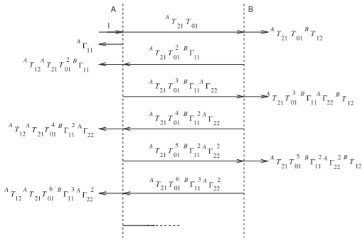
Figure \(\PageIndex{14}\): Bounce diagram of the transmission line network in Figure \(\PageIndex{12}\).
This example is similar to Example \(\PageIndex{4}\). Again, the transmission line network of Figure 2.5.1 is considered, but now the characteristic impedance of the first transmission line is not the same as the generator impedance and so the simplification used in the previous example can no longer be used. Now the generator has a Thevenin impedance \(Z_{1} = 40\:\Omega\) and source \(E = 5\text{ V}_{\text{peak}}\), connected to a one-quarter wavelength long line of characteristic impedance \(Z_{01} = 30\:\Omega\) that in turn is connected to an infinitely long line of characteristic impedance \(Z_{02} = 100\:\Omega\). The transmission lines are lossless. Two reference planes are shown in Figure 2.5.1. At reference plane \(\mathsf{1}\) the incident power is \(P_{I1}\) (the maximum available power from the source), the reflected power is \(P_{R1}\) and the transmitted power is \(P_{T1}\). \(P_{I2}\) (the maximum available power from \(Z_{01}\)), \(P_{R2}\), and \(P_{T2}\) are similar quantities at reference plane \(\mathsf{2}\). \(P_{I1},\: P_{R1},\: P_{T1},\: P_{I2},\: P_{R2},\) and \(P_{T2}\) are steady-state quantities.
- What is \(P_{I1}\)?
- What is \(P_{T2}\)?
- Determine \(P_{T1},\: P_{I2},\: P_{R1},\) and \(P_{R2}\).
Solution
One of the first things to note is that the infinitely long \(100\:\Omega\) transmission line is indistinguishable from a \(100\:\Omega\) resistor, so the reduced form of the problem is as shown below.
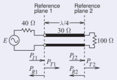
Figure \(\PageIndex{15}\)
- \(P_{I1}\) was calculated in Example \(\PageIndex{4}\) in Equation \(\eqref{eq:16}\):
\[\label{eq:41}P_{I1}=78.13\text{ mW} \]
\(P_{I1}\) is the available power from the source and this is the power that would be delivered to a load that is conjugately matched to the Thevenin equivalent source impedance. - The problem here is finding \(P_{T2}\). Recall that the powers here are steady-state quantities so that multiple reflections of, say, a pulse are not being considered. Since the system is lossless, the power delivered by the generator must be the power delivered to the infinitely long transmission line \(Z_{02}\) (i.e., \(P_{T2}\)). The telegrapher’s equation can be used to calculate the input impedance, \(Z_{\text{in}}\), of the two transmission line system; that is, the input impedance of \(Z_{01}\) from the generator end. However, a simpler way to find this impedance is to realize that the \(Z_{01}\) line is a \(\lambda/4\) transformer so that
\[\label{eq:42}Z_{01}=30\:\Omega=\sqrt{Z_{\text{in}}Z_{02}}=\sqrt{100Z_{\text{in}}} \]
and so
\[\label{eq:43}Z_{\text{in}}=9\:\Omega \]
The equivalent circuit is as shown below, where \(E\) is the original generator voltage of \(5\text{ V}\) and
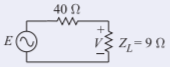
Figure \(\PageIndex{16}\)
\[\label{eq:44} V=\frac{9}{40+9}5=0.9184\text{ V} \]
The power delivered by the generator to the \(9\:\Omega\) load is
\[\label{eq:45}P_{T2}=\frac{1}{2}V^{2}/9=0.04686\text{ W}=46.86\text{ mW} \] - The power transmitted into the system at reference plane \(\mathsf{1}\), \(P_{T1}\), is the same as the power transmitted to the \(100\:\Omega\) load, as the first transmission line is lossless; that is,
\[\label{eq:46}P_{T1}=P_{T2}=46.86\text{ mW} \]
Also
\[\label{eq:47}P_{R1}=P_{I1}-P_{T1}=(78.13-46.86)\text{ mW}=31.27\text{ mW} \]
The two remaining quantities to determine are \(P_{I2}\) and \(P_{R2}\). There can be a number of interpretations of what these should be, but one thing that is certain is that
\[\label{eq:48}P_{T2}=P_{I2}-P_{R2}=46.86\text{ mW} \]
One interpretation that will be followed here is based on the equivalent circuit at reference plane \(\mathsf{2}\). Let \(Z_{\text{out}}\) be the impedance looking to the left from reference plane \(\mathsf{2}\). Again, using the property of a one-quarter wavelength long transmission line,
\[\label{eq:49}Z_{01}=30=\sqrt{Z_{\text{out}}\times 40} \]
and so
\[\label{eq:50}Z_{\text{out}}=Z_{01}^{2}/40=30^{2}/40=22.5\:\Omega \]
The equivalent circuit at reference plane \(\mathsf{2}\) is then
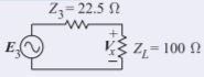
Figure \(\PageIndex{17}\)
Now determine \(V_{x}\) that results in a power \(P_{T2}\) being delivered to the \(100\:\Omega\) load, so
\[\label{eq:51}P_{T2}=\frac{1}{2}V_{x}^{2}/100=0.04686\text{ W} \]
and
\[\label{eq:52}V_{x}=3.06\text{ V} \]
From the circuit above,
\[\label{eq:53}V_{x}=\frac{100}{100+22.5}E_{3} \]
and so
\[\label{eq:54}E_{3}=3.75\text{ V} \]
The available power from this source is obtained by considering
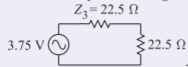
Figure \(\PageIndex{18}\)
The available power at reference plane \(\mathsf{2}\) is
\[\label{eq:55}P_{I2}=\frac{1}{2}\frac{(E_{3}/2)^{2}}{22.5}=\frac{1.875^{2}}{2\times 22.5} =0.07813\text{ W}=78.13\text{ mW} \]
From Equation \(\eqref{eq:48}\),
\[\label{eq:56}P_{R2}=P_{I2}-P_{T1}=(78.13-46.86)\text{ mW}=31.27\text{ mW} \]
Note that \(P_{R2}\) in Equation \(\eqref{eq:56}\) is the same as \(P_{R1}\) in Equation \(\eqref{eq:47}\), as expected.