
3.8: Amplifiers and RFICs
- Page ID
- 46047
\( \newcommand{\vecs}[1]{\overset { \scriptstyle \rightharpoonup} {\mathbf{#1}} } \)
\( \newcommand{\vecd}[1]{\overset{-\!-\!\rightharpoonup}{\vphantom{a}\smash {#1}}} \)
\( \newcommand{\id}{\mathrm{id}}\) \( \newcommand{\Span}{\mathrm{span}}\)
( \newcommand{\kernel}{\mathrm{null}\,}\) \( \newcommand{\range}{\mathrm{range}\,}\)
\( \newcommand{\RealPart}{\mathrm{Re}}\) \( \newcommand{\ImaginaryPart}{\mathrm{Im}}\)
\( \newcommand{\Argument}{\mathrm{Arg}}\) \( \newcommand{\norm}[1]{\| #1 \|}\)
\( \newcommand{\inner}[2]{\langle #1, #2 \rangle}\)
\( \newcommand{\Span}{\mathrm{span}}\)
\( \newcommand{\id}{\mathrm{id}}\)
\( \newcommand{\Span}{\mathrm{span}}\)
\( \newcommand{\kernel}{\mathrm{null}\,}\)
\( \newcommand{\range}{\mathrm{range}\,}\)
\( \newcommand{\RealPart}{\mathrm{Re}}\)
\( \newcommand{\ImaginaryPart}{\mathrm{Im}}\)
\( \newcommand{\Argument}{\mathrm{Arg}}\)
\( \newcommand{\norm}[1]{\| #1 \|}\)
\( \newcommand{\inner}[2]{\langle #1, #2 \rangle}\)
\( \newcommand{\Span}{\mathrm{span}}\) \( \newcommand{\AA}{\unicode[.8,0]{x212B}}\)
\( \newcommand{\vectorA}[1]{\vec{#1}} % arrow\)
\( \newcommand{\vectorAt}[1]{\vec{\text{#1}}} % arrow\)
\( \newcommand{\vectorB}[1]{\overset { \scriptstyle \rightharpoonup} {\mathbf{#1}} } \)
\( \newcommand{\vectorC}[1]{\textbf{#1}} \)
\( \newcommand{\vectorD}[1]{\overrightarrow{#1}} \)
\( \newcommand{\vectorDt}[1]{\overrightarrow{\text{#1}}} \)
\( \newcommand{\vectE}[1]{\overset{-\!-\!\rightharpoonup}{\vphantom{a}\smash{\mathbf {#1}}}} \)
\( \newcommand{\vecs}[1]{\overset { \scriptstyle \rightharpoonup} {\mathbf{#1}} } \)
\( \newcommand{\vecd}[1]{\overset{-\!-\!\rightharpoonup}{\vphantom{a}\smash {#1}}} \)
\(\newcommand{\avec}{\mathbf a}\) \(\newcommand{\bvec}{\mathbf b}\) \(\newcommand{\cvec}{\mathbf c}\) \(\newcommand{\dvec}{\mathbf d}\) \(\newcommand{\dtil}{\widetilde{\mathbf d}}\) \(\newcommand{\evec}{\mathbf e}\) \(\newcommand{\fvec}{\mathbf f}\) \(\newcommand{\nvec}{\mathbf n}\) \(\newcommand{\pvec}{\mathbf p}\) \(\newcommand{\qvec}{\mathbf q}\) \(\newcommand{\svec}{\mathbf s}\) \(\newcommand{\tvec}{\mathbf t}\) \(\newcommand{\uvec}{\mathbf u}\) \(\newcommand{\vvec}{\mathbf v}\) \(\newcommand{\wvec}{\mathbf w}\) \(\newcommand{\xvec}{\mathbf x}\) \(\newcommand{\yvec}{\mathbf y}\) \(\newcommand{\zvec}{\mathbf z}\) \(\newcommand{\rvec}{\mathbf r}\) \(\newcommand{\mvec}{\mathbf m}\) \(\newcommand{\zerovec}{\mathbf 0}\) \(\newcommand{\onevec}{\mathbf 1}\) \(\newcommand{\real}{\mathbb R}\) \(\newcommand{\twovec}[2]{\left[\begin{array}{r}#1 \\ #2 \end{array}\right]}\) \(\newcommand{\ctwovec}[2]{\left[\begin{array}{c}#1 \\ #2 \end{array}\right]}\) \(\newcommand{\threevec}[3]{\left[\begin{array}{r}#1 \\ #2 \\ #3 \end{array}\right]}\) \(\newcommand{\cthreevec}[3]{\left[\begin{array}{c}#1 \\ #2 \\ #3 \end{array}\right]}\) \(\newcommand{\fourvec}[4]{\left[\begin{array}{r}#1 \\ #2 \\ #3 \\ #4 \end{array}\right]}\) \(\newcommand{\cfourvec}[4]{\left[\begin{array}{c}#1 \\ #2 \\ #3 \\ #4 \end{array}\right]}\) \(\newcommand{\fivevec}[5]{\left[\begin{array}{r}#1 \\ #2 \\ #3 \\ #4 \\ #5 \\ \end{array}\right]}\) \(\newcommand{\cfivevec}[5]{\left[\begin{array}{c}#1 \\ #2 \\ #3 \\ #4 \\ #5 \\ \end{array}\right]}\) \(\newcommand{\mattwo}[4]{\left[\begin{array}{rr}#1 \amp #2 \\ #3 \amp #4 \\ \end{array}\right]}\) \(\newcommand{\laspan}[1]{\text{Span}\{#1\}}\) \(\newcommand{\bcal}{\cal B}\) \(\newcommand{\ccal}{\cal C}\) \(\newcommand{\scal}{\cal S}\) \(\newcommand{\wcal}{\cal W}\) \(\newcommand{\ecal}{\cal E}\) \(\newcommand{\coords}[2]{\left\{#1\right\}_{#2}}\) \(\newcommand{\gray}[1]{\color{gray}{#1}}\) \(\newcommand{\lgray}[1]{\color{lightgray}{#1}}\) \(\newcommand{\rank}{\operatorname{rank}}\) \(\newcommand{\row}{\text{Row}}\) \(\newcommand{\col}{\text{Col}}\) \(\renewcommand{\row}{\text{Row}}\) \(\newcommand{\nul}{\text{Nul}}\) \(\newcommand{\var}{\text{Var}}\) \(\newcommand{\corr}{\text{corr}}\) \(\newcommand{\len}[1]{\left|#1\right|}\) \(\newcommand{\bbar}{\overline{\bvec}}\) \(\newcommand{\bhat}{\widehat{\bvec}}\) \(\newcommand{\bperp}{\bvec^\perp}\) \(\newcommand{\xhat}{\widehat{\xvec}}\) \(\newcommand{\vhat}{\widehat{\vvec}}\) \(\newcommand{\uhat}{\widehat{\uvec}}\) \(\newcommand{\what}{\widehat{\wvec}}\) \(\newcommand{\Sighat}{\widehat{\Sigma}}\) \(\newcommand{\lt}{<}\) \(\newcommand{\gt}{>}\) \(\newcommand{\amp}{&}\) \(\definecolor{fillinmathshade}{gray}{0.9}\)Silicon RFICs exploit the high-density integration possible with silicon MOSFET transistors. These transistors can be fabricated with high levels of repeatability so that the transistors in differential designs can be closely matched. As well, the inherent compatibility with digital circuits enables digital control of RF circuits. As far as amplifiers are concerned, there are a few commonly used basic circuits that use complementary MOSFETs (nMOS and pMOS), that is, CMOS transistors. MOSFET differential amplifiers have been presented throughout this chapter. Other common CMOS circuits are shown in Figure \(\PageIndex{2}\). The transistors in all the circuits described here operate in the saturation region.
A cascode amplifier is shown in Figure \(\PageIndex{2}\)(a). There are two FETs, with the top FET acting as the drain load of the bottom FET. The gate of the top FET is held at ground so the voltage at the source of the top FET (and the drain of the bottom FET) is held at a nearly constant voltage. Thus the top FET presents a low-resistance load to the bottom FET. The voltage gain of the bottom FET is low, and this reduces the Miller effect capacitance, which is the effective input capacitance (being the gate-drain capacitance multiplied by the transistor voltage gain). The cascode topology increases the bandwidth of the circuit. Current gain, and hence power gain, is still realized by the bottom transistor. The voltage gain of the circuit depends on the resistance presented to the drain of the top transistor.
A variable gain cascode amplifier is shown in Figure \(\PageIndex{2}\)(b). This is similar to the cascode amplifier of Figure \(\PageIndex{2}\)(a), but now the voltage at
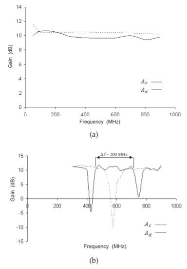
Figure \(\PageIndex{1}\): Measured common-mode gain, \(A_{c}\), and differential-mode gain, \(A_{d}\): (a) with inductor-based biasing circuit with lumped inductors of \(0.75\:\mu\text{H}\); and (b) with balun-like biasing circuit without lumped capacitors.
the gate of the top transistor, \(V_{G1}\), is selected so that a variable resistance is presented to the bottom transistor, thus the voltage gain of the circuit can be varied. This is a variable gain amplifier.
FET circuits are nearly always current biased, so circuits that realize current sources and current matching are particularly important. A single MOSFET can be used to realize a current source. If the gate-to-source voltage of a MOSFET is fixed, a near-constant current source is realized (see the drain-source current equation, Equation (1.3.17)). A differential amplifier circuit with a variable current source is shown in Figure \(\PageIndex{2}\)(d). What is particularly interesting is that the transistor controlling the bias to the current source can be part of a digital circuit, enabling digital control of the analog circuit bias. The concept can be replicated by replacing \(M_{1}\) by multiple transistors in parallel with each transistor having a binary signal at the gate. This is a fundamental component in the digital control of analog circuits, including RFICs. For example, modern RFICs incorporate digitally controlled trimming of RFICs to achieve, for example, enhanced \(IQ\) balance of quadrature modulators.
Another circuit that controls current in an RFIC is the current mirror shown in Figure \(\PageIndex{2}\)(c). In this circuit, \(I_{1} = I_{2}\), as the gate-source voltages of transistors \(M_{1}\) and \(M_{2}\) are the same. The drain-gate connection of \(M_{1}\) ensures
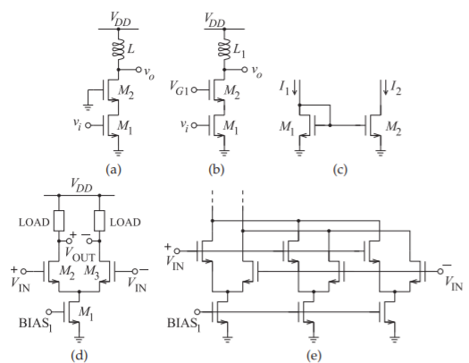
Figure \(\PageIndex{2}\): MOS analog circuits: (a) cascode amplifier; (b) variable gain cascode amplifier; (c) current mirror; (d) differential pair; (e) multi-tanh triplet implementation of a differential pair providing enhanced linearity.
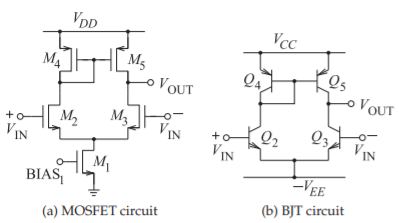
Figure \(\PageIndex{3}\): Differential pair circuits each with a current mirror.
that the gate-source voltage will be whatever is needed to support the current \(I_{1}\) derived from the rest of the circuit.
A CMOS differential amplifier with a current mirror load is shown in Figure \(\PageIndex{3}\)(a). In this configuration the current mirror presents a high differential impedance. If the load impedance presented to the terminal, labeled \(V_{\text{OUT}}\), is less than this load, then the current mirror-loaded differential amplifier realizes a single-ended output while having the essential functionality of a differential circuit to reject common-mode signals. There is a price to pay for this functionality. The circuit of Figure \(\PageIndex{3}\)(a) has three drain-source voltage drops between the rails. This reduces the available
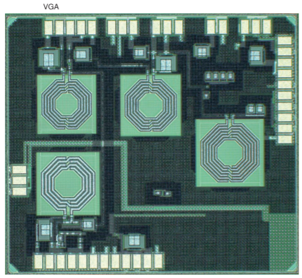
Figure \(\PageIndex{4}\): Photomicrograph of a \(90\text{ nm}\) CMOS WCDMA transmitter showing (MIXER) the up-conversion mixer and quadrature LO divider; (VGA) the cascode variable gain amplifier; and the twostage driver amplifier with \(9.6\text{ dBm}\) output power. Die size is \(1.1\text{ mm }\times\: 1.4\text{ mm}\). After Yang [21], and Yang and Gard [12]. Copyright K. Gard and X. Yang, used with permission.
voltage swing. This is one of the major problems encountered with RFICs, as the supply voltage is dictated by the relatively low supply voltages that can be supported in a process that is optimized for low-voltage digital circuits. A current mirror can also be realized using BJTs with the BJT-based current mirror-loaded differential pair shown in Figure \(\PageIndex{3}\)(b) as an example.
Mathematically the simplified input-output characteristic of a MOSFET is essentially a quadratic (see Equation (1.3.17)). It is a challenge to take such fundamental algebraic models and derive the equations that describe the operation of a complete circuit; a challenge that must be addressed in the synthesis of a circuit with specified distortion and noise performance. It can be shown that the relationship between the drain current and the drain-source voltage has the form of a tanh function [10]. In terms of the transconductance, \(g_{m}\), it appears as a quadratic-like function with a peak value at a drain voltage that is controlled by the \(W/L\) ratio. By putting several differential pairs in parallel, with each pair having staggered \(W/L\) ratios, a compound differential amplifier with enhanced linearity can be realized [11, 12]. This circuit is known as a multi-tanh differential pair. A triplet multi-tanh differential pair is shown in Figure \(\PageIndex{2}\)(e). Detailed RFIC design involves the algebraic derivation of the required conditions. This network synthesis applied to RFICs is explored in numerous references [13, 14, 15, 16, 17, 18, 19, 20] as well as a large number of papers on RFIC design. Synthesis to control distortion and noise is at the heart of RFIC design. Collecting novel circuit topologies, and the techniques to synthesize them (e.g. from conference and journal papers and patents), is an essential part of RFIC design; which is not that different from the process for all other forms of circuit design.
Figure \(\PageIndex{4}\) is a photomicrograph of a \(90\text{ nm}\) WCDMA transmitter. The design consists of three blocks: an up-converting mixer (MIXER), a variable gain cascode amplifier (VGA), and a two-stage driver amplifier. The
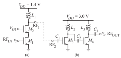
Figure \(\PageIndex{5}\): Three-stage amplifier of the WCDMA receiver shown in Figure \(\PageIndex{4}\): (a) a variable gain cascode amplifier; and (b) the two-stage driver amplifier. After Yang [21], and Yang and Gard [12]. Copyright K. Gard and X. Yang, used with permission.
schematic of the output amplifier stages is shown in Figure \(\PageIndex{5}\). The variable gain amplifier, the VGA block, is a cascode amplifier with variable biasing of the top FET in the cascode to realize a variable gain. Each of the amplifiers in the two-stage driver amplifier has a different \(V_{DD}\) so that the nonlinearities of the two stages can be designed to cancel, and thus the overall performance of the driver amplifier is linearized [12, 21].