
1.2: The Closed-loop Gain of an Operational Amplifier
- Page ID
- 58434

\( \newcommand{\vecs}[1]{\overset { \scriptstyle \rightharpoonup} {\mathbf{#1}} } \)
\( \newcommand{\vecd}[1]{\overset{-\!-\!\rightharpoonup}{\vphantom{a}\smash {#1}}} \)
\( \newcommand{\id}{\mathrm{id}}\) \( \newcommand{\Span}{\mathrm{span}}\)
( \newcommand{\kernel}{\mathrm{null}\,}\) \( \newcommand{\range}{\mathrm{range}\,}\)
\( \newcommand{\RealPart}{\mathrm{Re}}\) \( \newcommand{\ImaginaryPart}{\mathrm{Im}}\)
\( \newcommand{\Argument}{\mathrm{Arg}}\) \( \newcommand{\norm}[1]{\| #1 \|}\)
\( \newcommand{\inner}[2]{\langle #1, #2 \rangle}\)
\( \newcommand{\Span}{\mathrm{span}}\)
\( \newcommand{\id}{\mathrm{id}}\)
\( \newcommand{\Span}{\mathrm{span}}\)
\( \newcommand{\kernel}{\mathrm{null}\,}\)
\( \newcommand{\range}{\mathrm{range}\,}\)
\( \newcommand{\RealPart}{\mathrm{Re}}\)
\( \newcommand{\ImaginaryPart}{\mathrm{Im}}\)
\( \newcommand{\Argument}{\mathrm{Arg}}\)
\( \newcommand{\norm}[1]{\| #1 \|}\)
\( \newcommand{\inner}[2]{\langle #1, #2 \rangle}\)
\( \newcommand{\Span}{\mathrm{span}}\) \( \newcommand{\AA}{\unicode[.8,0]{x212B}}\)
\( \newcommand{\vectorA}[1]{\vec{#1}} % arrow\)
\( \newcommand{\vectorAt}[1]{\vec{\text{#1}}} % arrow\)
\( \newcommand{\vectorB}[1]{\overset { \scriptstyle \rightharpoonup} {\mathbf{#1}} } \)
\( \newcommand{\vectorC}[1]{\textbf{#1}} \)
\( \newcommand{\vectorD}[1]{\overrightarrow{#1}} \)
\( \newcommand{\vectorDt}[1]{\overrightarrow{\text{#1}}} \)
\( \newcommand{\vectE}[1]{\overset{-\!-\!\rightharpoonup}{\vphantom{a}\smash{\mathbf {#1}}}} \)
\( \newcommand{\vecs}[1]{\overset { \scriptstyle \rightharpoonup} {\mathbf{#1}} } \)
\( \newcommand{\vecd}[1]{\overset{-\!-\!\rightharpoonup}{\vphantom{a}\smash {#1}}} \)
As mentioned in the introduction, most operational-amplifier connec tions involve feedback. Therefore the user is normally interested in deter mining the closed-loop gain or closed-loop transferfunctionof the amplifier, which results when feedback is included. As we shall see, this quantity can be made primarily dependent on the characteristics of the feedback ele ments in many cases of interest.
A prerequisite for the material presented in the remainder of this book is the ability to determine the gain of the amplifier-feedback network com bination in simple connections. The techniques used to evaluate closed-loop gain are outlined in this section.

Closed-Loop Gain Calculation
The symbol used to designate an operational amplifier is shown in Figure 1.1. The amplifier shown has a differential input and a single output. The input terminals marked - and + are called the inverting and the non-inverting input terminals respectively. The implied linear-region relationship among input and output variables(*) is
* The notation used to designate system variables consists of a symbol and a subscript. This combination serves not only as a label, but also to identify the nature of the quantity as follows:
Total instantaneous variables:
lower-case symbols with upper-case subscripts.
Quiescent or operating-point variables:
upper-case symbols with upper-case subscripts.
Incremental instantaneous variables:
lower-case symbols with lower-case subscripts.
Complex amplitudes or Laplace transforms of incremental variables:
upper-case symbols with lower-case subscripts.
Using this notation we would write \(v1 = V_1 + v_i\), indicating that the instantaneous value of vi consists of a quiescent plus an incremental component. The transform of vi is Vi. The notation \(V_i (s)\) is often used to reinforce the fact that \(V_i\) is a function of the complex variable \(s\).
\[V_o = a(V_a - V_b) \nonumber \]
The quantity a in this equation is the open-loop gain or open-loop transfer function of the amplifier. (Note that a gain of a is assumed, even if it is not explicitly indicated inside the amplifier symbol.) The dynamics normally associated with this transfer function are frequently emphasized by writing \(a(s)\).
It is also necessary to provide operating power to the operational ampli fier via power-supply terminals. Many operational amplifiers use balanced (equal positive and negative) supply voltages. The various signals are usually referenced to the common ground connection of these power supplies. The power connections are normally not included in diagrams in tended only to indicate relationships among signal variables, since eliminating these connections simplifies the diagram.
Although operational amplifiers are used in a myriad of configurations, many applications are variations of either the inverting connection (Figure1.2a) or the noninverting connection (Figure 1.2b). These connections com bine the amplifier with impedances that provide feedback.
The closed-loop transfer function is calculated as follows for the invert ing connection. Because of the reference polarity chosen for the inter mediate variable \(V_a\),
\[V_o = -aV_a \nonumber \]


where it has been assumed that the output voltage of the amplifier is not modified by the loading of the \(Z_1-Z_2\) network. If the input impedance of the amplifier itself is high enough so that the \(Z_1 - Z_2\) network is not loaded significantly, the voltage \(V_a\) is
\[V_a = \left ( \dfrac{Z_2}{Z_1 + Z_2} \right ) V_i + \left ( \dfrac{Z_1}{Z_1 + Z_2} \right ) V_o \nonumber \]
Combining Equations 1.2 and 1.3 yields
\[V_o = -\left ( \dfrac{a Z_2}{Z_1 + Z_2} \right ) V_i - \left ( \dfrac{a Z_1}{Z_1 + Z_2} \right ) V_o \nonumber \]
or, solving for the closed-loop gain,
\[\dfrac{V_o}{V_i} = \dfrac{-aZ_2/(Z_1 + Z_2)}{1 + [aZ_1/(Z_1 + Z_2)]} \nonumber \]
The condition that is necessary to have the closed-loop gain depend primarily on the characteristics of the \(Z_i-Z_2\) network rather than on the performance of the amplifier itself is easily determined from Equation 1.5. At any frequency \(\omega\) where the inequality \(|a(j\omega) Z_1 (j\omega)/[Z_1(j\omega) + Z_2 (j\omega)]| \gg 1\) is satisfied, Equation 1.5 reduces to
\[\dfrac{V_o (j\omega)}{V_i (j\omega)} \simeq -\dfrac{Z_2 (j\omega)}{Z_1 (j\omega)} \nonumber \]
The closed-loop gain calculation for the noninverting connection is similar. If we assume negligible loading at the amplifier input and output,
\[V_o = a(V_i - V_a) = aV_i - \left ( \dfrac{aZ_1}{Z_1 + Z_2} \right ) V_o \nonumber \]
or
\[\dfrac{V_o}{V_i} = \dfrac{a}{1+[aZ_1/(Z_1 + Z_2)]} \nonumber \]
This expression reduces to
\[\dfrac{V_o (j\omega)}{V_i (j\omega)} \simeq \dfrac{Z_1 (j\omega) + Z_2 (j\omega)}{Z_1 (j\omega)} \nonumber \]
when \(|a(j \omega) Z_1 (j \omega)/[Z_1 (j \omega) + Z_2 (j \omega)]| \gg 1\).
The quantity
\[L = \dfrac{-aZ_1}{Z_1 + Z_2} \nonumber \]
is the loop transmission for either of the connections of Figure 1.2. The loop transmission is of fundamental importance in any feedback system because it influences virtually all closed-loop parameters of the system. For ex ample, the preceding discussion shows that if the magnitude of loop trans mission is large, the closed-loop gain of either the inverting or the non- inverting amplifier connection becomes virtually independent of a. This relationship is valuable, since the passive feedback components that deter mine closed-loop gain for large loop-transmission magnitude are normally considerably more stable with time and environmental changes than is the open-loop gain a.
The loop transmission can be determined by setting the inputs of a feed back system to zero and breaking the signal path at any point inside the feedback loop.(There are practical difficulties, such as insuring that the various elements in the loop remain in their linear operating regions and that loading ismaintained. These difficulties complicate the determination of the loop transmission in physical systems. Therefore, the technique described here should be considered a conceptual experiment. Methods that are useful for actual hardware are introduced in later sections.) The loop transmission is the ratio of the signal returned by the loop to a test applied at the point where the loop is opened. Figure 1.3 indicates one way to determine the loop transmission for the connections of Figure 1.2. Note that the topology shown is common to both the inverting and the noninverting connection when input points are grounded.
It is important to emphasize the difference between the loop transmission, which is dependent on properties of both the feedback elements and the operational amplifier, and the open-loop gain of the operational amplifier itself.
Ideal Closed-Loop Gain
Detailed gain calculations similar to those of the last section are always possible for operational-amplifier connections. However, operational ampli fiers are frequently used in feedback connections where loop characteristics are such that the closed-loop gain is determined primarily by the feedback elements. Therefore, approximations that indicate the idealclosed-loopgain or the gain that results with perfect amplifier characteristics simplify the analysis or design of many practical connections.
It is possible to calculate the ideal closed-loop gain assuming only two conditions (in addition to the implied condition that the amplifier-feedback network combination is stable(Stability is discussed in detail in Chapter 4.)) are satisfied.
1. A negligibly small differential voltage applied between the two input terminals of the amplifier is sufficient to produce any desired output voltage.

2. The current required at either amplifier terminal is negligibly small.
The use of these assumptions to calculate the ideal closed-loop gain is first illustrated for the inverting amplifier connection (Figure 1.2a). Since the noninverting amplifier input terminal is grounded in this connection, condition 1 implies that
\[V_a \simeq 0 \nonumber \]
Kirchhoff's current law combined with condition 2 shows that
\[I_a + I_b \simeq 0 \nonumber \]
With Equation 1.11 satisfied, the currents \(I_a\) and \(I_b\) are readily determined in terms of the input and output voltages.
\[I_a \simeq \dfrac{V_i}{Z_1} \nonumber \]
\[I_b \simeq \dfrac{V_o}{Z_2} \nonumber \]
Combining Equations 1.12, 1.13, and 1.14 and solving for the ratio of \(V_o\) to \(V_i\) yields the ideal closed-loop gain
\[\dfrac{V_o}{V_i} = -\dfrac{Z_2}{Z_1} \nonumber \]
The technique used to determine the ideal closed-loop gain is called the virtual-ground method when applied to the inverting connection, since in this case the inverting input terminal of the operational amplifier is assumed to be at ground potential.
The noninverting amplifier (Figure 1.2b) provides a second example of ideal-gain determination. Condition 2 insures that the voltage \(V_a\) is not influenced by current at the inverting input. Thus,
\[V_a \simeq \dfrac{Z_1}{Z_1 +Z_2} V_o \nonumber \]
Since condition 1 requires equality between \(V_a\), and \(V_i\), the ideal closed-loop gain is
\[\dfrac{V_o}{V_i} = \dfrac{Z_1 + Z_2}{Z_1} \nonumber \]
The conditions can be used to determine ideal values for characteristics other than gain. Consider, for example, the input impedance of the two amplifier connections shown in Figure 1.2. In Figure 1.2a, the inverting input terminal and, consequently, the right-hand end of impedance \(Z_1\), is at ground potential if the amplifier characteristics are ideal. Thus the input impedance seen by the driving source is simply \(Z_1\). The input source is connected directly to the noninverting input of the operational amplifier in the topology of Figure 1.2b. If the amplifier satisfies condition 2 and has negligible input current required at this terminal, the impedance loading the signal source will be very high. The noninverting connection is often used as a buffer amplifier for this reason.
The two conditions used to determine the ideal closed-loop gain are deceptively simple in that a complex combination of amplifier characteris tics are required to insure satisfaction of these conditions. Consider the first condition. High open-loop voltage gain at anticipated operating fre quencies is necessary but not sufficient to guarantee this condition. Note that gain at the frequency of interest is necessary, while the high open-loop gain specified by the manufacturer is normally measured at d-c. This speci fication is somewhat misleading, since the gain may start to decrease at a frequency on the order of one hertz or less.
In addition to high open-loop gain, the amplifier must have low voltage offset(Offset and other problems with d-c amplifiers are discussed in Chapter 7. ) referred to the input to satisfy the first condition. This quantity, defined as the voltage that must be applied between the amplifier input terminals to make the output voltage zero, usually arises because of mis matches between various amplifier components.
Surprisingly, the incremental input impedance of an operational ampli fier often has relatively little effect on its input current, since the voltage that appears across this impedance is very low if condition 1 is satisfied. A more important contribution to input current often results from the bias current that must be supplied to the amplifier input transistors.
Many of the design techniques that are used in an attempt to combine the two conditions necessary to approach the ideal gain are described in sub sequent sections.
The reason that the satisfaction of the two conditions introduced earlier guarantees that the actual closed-loop gain of the amplifier approaches the ideal value is because of the negative feedback associated with operational-amplifier connections. Assume, for example, that the actual voltage out of the inverting-amplifier connection shown in Figure 1.2a is more positive than the value predicted by the ideal-gain relationship for a particular input signal level. In this case, the voltage \(V_a\) will be positive, and this positive voltage applied to the inverting input terminal of the amplifier drives the output voltage negative until equilibrium is reached. This reasoning shows that it is actually the negative feedback that forces the voltage between the two input terminals to be very small.

Alternatively, consider the situation that results if positive feedback is used by interchanging the connections to the two input terminals of the amplifier. In this case, the voltage \(V_a\) is again zero when \(V_o\) and \(V_i\) are related by the ideal closed-loop gain expression. However, the resulting equilibrium is unstable, and a small perturbation from the ideal output voltage results in this voltage being driven further from the ideal value until the amplifier saturates. The ideal gain is not achieved in this case in spite of perfect amplifier characteristics because the connection is unstable. As we shall see, negative feedback connections can also be unstable. The ideal gain of these unstable systems is meaningless because they oscillate, producing an output signal that is often nearly independent of the input signal.
Examples
The technique introduced in the last section can be used to determine the ideal closed-loop transfer function of any operational-amplifier connection. The summing amplifier shown in Figure 1.4 illustrates the use of this technique for a connection slightly more complex than the two basic amplifiers discussed earlier.
Since the inverting input terminal of the amplifier is a virtual ground, the currents can be determined as
\[\begin{array} {rcl} {I_{i1}} & = & {\dfrac{V_{i1}}{Z_{i1}}} \\ {I_{i2}} & = & {\dfrac{V_{i2}}{Z_{i2}}} \\ {} & \cdot & {} \\ {} & \cdot & {} \\ {} & \cdot & {} \\ {I_{iN}} & = & {\dfrac{V_{iN}}{Z_{iN}}} \\ {I_f} & = & {\dfrac{V_o}{Z_f}} \end{array} \nonumber \]
These currents must sum to zero in the absence of significant current at the inverting input terminal of the amplifier. Thus
\[I_{i1} + I_{i2} + \cdots + I_{iN} + I_f = 0 \nonumber \]
Combining Equations 1.18 and 1.19 shows that
\[V_o = -\dfrac{Z_f}{Z_{i1}} V_{i1} - \dfrac{Z_f}{Z_{i2}} V_{i2} - \cdots - \dfrac{Z_f}{Z_{iN}} V_{iN} \nonumber \]
We see that this amplifier, which is an extension of the basic inverting- amplifier connection, provides an output that is the weighted sum of several input voltages.
Summation is one of the "operations" that operational amplifiers per form in analog computation. A subsequent development (Section 12.3) will
show that if the operations of gain, summation, and integration are com bined, an electrical network that satisfies any linear, ordinary differential equation can be constructed. This technique is the basis for analog com putation.
Integrators required for analog computation or for any other application can be constructed by using an operational amplifier in the inverting con nection (Figure 1.2a) and making impedance \(Z_2\) a capacitor \(C\) and impedance \(Z_1\) a resistor \(R\). In this case, Equation 1.15 shows that the ideal closrd-loop transfer function is
\[\dfrac{V_o (s)}{V_i (s)} = -\dfrac{Z_2 (s)}{Z_1 (s)} = -\dfrac{1}{RCs} \nonumber \]
so that the connection functions as an inverting integrator.
It is also possible to construct noninverting integrators using an operational amplifier connected as shown in Figure 1.5. This topology precedes a noninverting amplifier with a low-pass filter. The ideal transfer function from the noninverting input of the amplifier to its output is (see Equation 1.17)
\[\dfrac{V_o (s)}{V_a (s)} = \dfrac{RVs + 1}{RCs} \nonumber \]
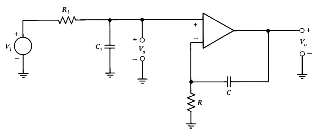

Since the conditions for an ideal operational amplifier preclude input current, the transfer function from \(V_i\) to \(V_a\) can be calculated with no loading, and in this case
\[\dfrac{V_a (s)}{V_i (s)} = \dfrac{1}{R_1 C_1 s + 1} \nonumber \]
Combining Equations 1.22 and 1.23 shows that the ideal closed-loop gain is
\[\dfrac{V_o (s)}{V_i (s)} = \left [\dfrac{1}{R_1 C_1s + 1} \right ] \left [\dfrac{RCs + 1}{RCs} \right ] \nonumber \]
If the two time constants in Equation 1.24 are made equal, noninverting inte gration results.
The comparison between the two integrator connections hints at the possibility of realizing most functions via either an inverting or a non-inverting connection. Practical considerations often recommend one ap proach in preference to the other. For example, the noninverting integrator requires more external components than does the inverting version. This difference is important because the high-quality capacitors required for accurate integration are often larger and more expensive than the opera tional amplifier that is used.
The examples considered up to now have involved only linear elements, at least if it is assumed that the operational amplifier remains in its linear
operating region. Operational amplifiers are also frequently used in intentionally nonlinear connections. One possibility is the circuit shown in Figure1.6.(Note that the notation for the variables used in this case combines lower-case variables with upper-case subscripts, indicating the total instantaneous signals necessary to describe the anticipated nonlinear relationships.) It is assumed that the diode current-voltage relationship is
\[i_D = I_S (e^{qv_D/kT} - 1) \nonumber \]
where \(I_s\) is a constant dependent on diode construction, \(q\) is the charge of an electron, \(k\) is Boltzmann's constant, and \(T\) is the absolute temperature. If the voltage at the inverting input of the amplifier is negligibly small, the diode voltage is equal to the output voltage. If the input current is negligibly small, the diode current and the current \(i_R\) sum to zero. Thus, if these two conditions are satisfied,
\[-\dfrac{v_I}{R} = I_S (e^{qv_O/kT} - 1) \nonumber \]
Consider operation with a positive input voltage. The maximum negative value of the diode current is limited to \(-I_s\). If \(v_I/R > I_S\), the current through the reverse-biased diode cannot balance the current \(I_R\). Accordingly, the amplifier output voltage is driven negative until the amplifier saturates. In this case, the feedback loop cannot keep the voltage at the inverting amplifier input near ground because of the limited current that the diode can conduct in the reverse direction. The problem is clearly not with the amplifier, since no solution exists to Equation 1.26 for sufficiently positive values of \(v_I\).
This problem does not exist with negative values for \(v_I\). If the magnitude of iR is considerably larger than Is (typical values for Is are less than \(10^{-9}\) A), Equation 1.26 reduces to
\[-\dfrac{v_I}{R} \simeq I_S e^{qv_O/kT} \nonumber \]
or
\[v_O \simeq \dfrac{kT}{q} \ln \left (\dfrac{-v_I}{RI_S} \right ) \nonumber \]
Thus the circuit provides an output voltage proportional to the log of the magnitude of the input voltage for negative inputs.