
7.3: THE DIFFERENTIAL AMPLIFIER
- Page ID
- 58459
\( \newcommand{\vecs}[1]{\overset { \scriptstyle \rightharpoonup} {\mathbf{#1}} } \)
\( \newcommand{\vecd}[1]{\overset{-\!-\!\rightharpoonup}{\vphantom{a}\smash {#1}}} \)
\( \newcommand{\dsum}{\displaystyle\sum\limits} \)
\( \newcommand{\dint}{\displaystyle\int\limits} \)
\( \newcommand{\dlim}{\displaystyle\lim\limits} \)
\( \newcommand{\id}{\mathrm{id}}\) \( \newcommand{\Span}{\mathrm{span}}\)
( \newcommand{\kernel}{\mathrm{null}\,}\) \( \newcommand{\range}{\mathrm{range}\,}\)
\( \newcommand{\RealPart}{\mathrm{Re}}\) \( \newcommand{\ImaginaryPart}{\mathrm{Im}}\)
\( \newcommand{\Argument}{\mathrm{Arg}}\) \( \newcommand{\norm}[1]{\| #1 \|}\)
\( \newcommand{\inner}[2]{\langle #1, #2 \rangle}\)
\( \newcommand{\Span}{\mathrm{span}}\)
\( \newcommand{\id}{\mathrm{id}}\)
\( \newcommand{\Span}{\mathrm{span}}\)
\( \newcommand{\kernel}{\mathrm{null}\,}\)
\( \newcommand{\range}{\mathrm{range}\,}\)
\( \newcommand{\RealPart}{\mathrm{Re}}\)
\( \newcommand{\ImaginaryPart}{\mathrm{Im}}\)
\( \newcommand{\Argument}{\mathrm{Arg}}\)
\( \newcommand{\norm}[1]{\| #1 \|}\)
\( \newcommand{\inner}[2]{\langle #1, #2 \rangle}\)
\( \newcommand{\Span}{\mathrm{span}}\) \( \newcommand{\AA}{\unicode[.8,0]{x212B}}\)
\( \newcommand{\vectorA}[1]{\vec{#1}} % arrow\)
\( \newcommand{\vectorAt}[1]{\vec{\text{#1}}} % arrow\)
\( \newcommand{\vectorB}[1]{\overset { \scriptstyle \rightharpoonup} {\mathbf{#1}} } \)
\( \newcommand{\vectorC}[1]{\textbf{#1}} \)
\( \newcommand{\vectorD}[1]{\overrightarrow{#1}} \)
\( \newcommand{\vectorDt}[1]{\overrightarrow{\text{#1}}} \)
\( \newcommand{\vectE}[1]{\overset{-\!-\!\rightharpoonup}{\vphantom{a}\smash{\mathbf {#1}}}} \)
\( \newcommand{\vecs}[1]{\overset { \scriptstyle \rightharpoonup} {\mathbf{#1}} } \)
\(\newcommand{\longvect}{\overrightarrow}\)
\( \newcommand{\vecd}[1]{\overset{-\!-\!\rightharpoonup}{\vphantom{a}\smash {#1}}} \)
\(\newcommand{\avec}{\mathbf a}\) \(\newcommand{\bvec}{\mathbf b}\) \(\newcommand{\cvec}{\mathbf c}\) \(\newcommand{\dvec}{\mathbf d}\) \(\newcommand{\dtil}{\widetilde{\mathbf d}}\) \(\newcommand{\evec}{\mathbf e}\) \(\newcommand{\fvec}{\mathbf f}\) \(\newcommand{\nvec}{\mathbf n}\) \(\newcommand{\pvec}{\mathbf p}\) \(\newcommand{\qvec}{\mathbf q}\) \(\newcommand{\svec}{\mathbf s}\) \(\newcommand{\tvec}{\mathbf t}\) \(\newcommand{\uvec}{\mathbf u}\) \(\newcommand{\vvec}{\mathbf v}\) \(\newcommand{\wvec}{\mathbf w}\) \(\newcommand{\xvec}{\mathbf x}\) \(\newcommand{\yvec}{\mathbf y}\) \(\newcommand{\zvec}{\mathbf z}\) \(\newcommand{\rvec}{\mathbf r}\) \(\newcommand{\mvec}{\mathbf m}\) \(\newcommand{\zerovec}{\mathbf 0}\) \(\newcommand{\onevec}{\mathbf 1}\) \(\newcommand{\real}{\mathbb R}\) \(\newcommand{\twovec}[2]{\left[\begin{array}{r}#1 \\ #2 \end{array}\right]}\) \(\newcommand{\ctwovec}[2]{\left[\begin{array}{c}#1 \\ #2 \end{array}\right]}\) \(\newcommand{\threevec}[3]{\left[\begin{array}{r}#1 \\ #2 \\ #3 \end{array}\right]}\) \(\newcommand{\cthreevec}[3]{\left[\begin{array}{c}#1 \\ #2 \\ #3 \end{array}\right]}\) \(\newcommand{\fourvec}[4]{\left[\begin{array}{r}#1 \\ #2 \\ #3 \\ #4 \end{array}\right]}\) \(\newcommand{\cfourvec}[4]{\left[\begin{array}{c}#1 \\ #2 \\ #3 \\ #4 \end{array}\right]}\) \(\newcommand{\fivevec}[5]{\left[\begin{array}{r}#1 \\ #2 \\ #3 \\ #4 \\ #5 \\ \end{array}\right]}\) \(\newcommand{\cfivevec}[5]{\left[\begin{array}{c}#1 \\ #2 \\ #3 \\ #4 \\ #5 \\ \end{array}\right]}\) \(\newcommand{\mattwo}[4]{\left[\begin{array}{rr}#1 \amp #2 \\ #3 \amp #4 \\ \end{array}\right]}\) \(\newcommand{\laspan}[1]{\text{Span}\{#1\}}\) \(\newcommand{\bcal}{\cal B}\) \(\newcommand{\ccal}{\cal C}\) \(\newcommand{\scal}{\cal S}\) \(\newcommand{\wcal}{\cal W}\) \(\newcommand{\ecal}{\cal E}\) \(\newcommand{\coords}[2]{\left\{#1\right\}_{#2}}\) \(\newcommand{\gray}[1]{\color{gray}{#1}}\) \(\newcommand{\lgray}[1]{\color{lightgray}{#1}}\) \(\newcommand{\rank}{\operatorname{rank}}\) \(\newcommand{\row}{\text{Row}}\) \(\newcommand{\col}{\text{Col}}\) \(\renewcommand{\row}{\text{Row}}\) \(\newcommand{\nul}{\text{Nul}}\) \(\newcommand{\var}{\text{Var}}\) \(\newcommand{\corr}{\text{corr}}\) \(\newcommand{\len}[1]{\left|#1\right|}\) \(\newcommand{\bbar}{\overline{\bvec}}\) \(\newcommand{\bhat}{\widehat{\bvec}}\) \(\newcommand{\bperp}{\bvec^\perp}\) \(\newcommand{\xhat}{\widehat{\xvec}}\) \(\newcommand{\vhat}{\widehat{\vvec}}\) \(\newcommand{\uhat}{\widehat{\uvec}}\) \(\newcommand{\what}{\widehat{\wvec}}\) \(\newcommand{\Sighat}{\widehat{\Sigma}}\) \(\newcommand{\lt}{<}\) \(\newcommand{\gt}{>}\) \(\newcommand{\amp}{&}\) \(\definecolor{fillinmathshade}{gray}{0.9}\)The highly predictable temperature coefficient of the base-to-emitter voltage of a bipolar transistor offers the possibility that some type of compensation can be used to produce low-drift amplifiers. It is evident that the use of one transistor junction to compensate for voltage variations of a second similar junction should provide excellent results since both devices vary in a similar way. This section describes a connection that exploits the
characteristics of a pair of bipolar transistors to provide low drift combined with several other useful features.
Topology
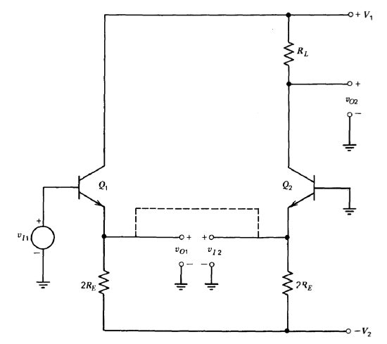
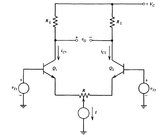
Consider the connection shown in Figure 7.3. Here transistor \(Q_2\) is connected as a common-base amplifier, while transistor \(Q_1\) is connected as an emitter follower. Assume that initially \(v_{I1} = 0\), that the two transistors are at the same temperature and that they are matched in the sense that they have identical saturation currents. In this case the voltages at the emitters of the two transistors will be equal, or \(v_{O1} = v_{I2}\). The connection shown as a dotted line can then be completed with no change in any voltage level. If the magnitude of the voltage \(V_2\) is much larger than anticipated variations in base-to-emitter voltage, the current through parallel resistor combination is virtually temperature independent. The matched transistor characteristics insure that this constant current divides equally between the two transistors. If we also assume that the common-base current gain of transistor \(Q_2\) is one, changes in temperature result in negligible changes in the collector current of this device. Thus the drift referred to the input of this connection can be close to zero. In addition to providing temperature compensation, the current gain and input resistance of transistor \(Q_1\) increases the input-resistance of the circuit by a factor of \(2\beta\) above that seen at the emitter of \(Q_2\).
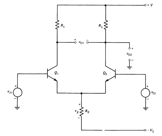
The circuit that results when the dotted connection in Figure 7.3 is completed is shown in Figure 7.4. The inherent symmetry of the differential amplifier has been emphasized by including a collector-load resistor for \(Q_1\) and permitting input signals to be applied to either base. A second output signal is indicated between the collectors of the two transistors in Figure 7.4, so that both differential(between collector) or single-ended(either collector to ground) outputs are available.
Gain
The output of the circuit of Figure 7.4 for any particular input voltage can be calculated by the usual methods. However, an alternative and useful analytic technique is available(An essentially identical analysis is given for vacuum-tube differential amplifiers in T. S. Gray, Applied Electronics, 2nd Ed., Wiley, New York, 1954, pages 504-509.) that simplifies the calculations and gives greater insight into the operation of the circuit. The gain of the circuit is calculated for two particular types of inputs, a differential input with \(v_{I1} = v_{I2}\), and a common-mode input with \(v_{I1} = v_{I2}\).
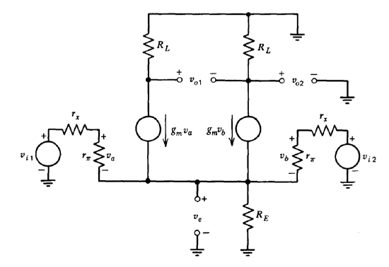
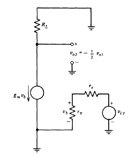
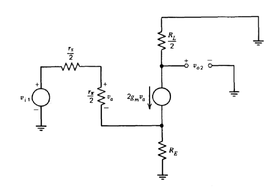
Figure 7.5 shows a schematic where the transistors have been replaced by appropriate, identical circuit models. Consider initially a pure differential input, of sufficiently small size so that the linear-region model remains valid. It is easily shown that in this case the voltage ve does not change and that the common emitter connection may therefore be considered an incrementally grounded point. The incremental model for either half circuit reduces to that shown in Figure 7.6. The incremental gain to the single- ended output, \(v_{o2}\), is simply that of a common-emitter amplifier:
\[\dfrac{v_{o2}}{v_{i2}}|_{v_{i1} = -v_{i2}} = \dfrac{-g_m R_L r_{\pi}}{r_x + r_{\pi}} \nonumber \]
The differential output component of \(v_{o1}\) for the left-hand half circuit is identical in magnitude but opposite in sign to that of the right-hand half circuit; therefore, \(v_{o2} = -\tfrac{1}{2} v_{o1}\). The incremental gain to a differential out put is then
\[\dfrac{v_{o1}}{v_{i2}}|_{v_{i1} = -v_{i2}} = \dfrac{2g_m R_L r_{\pi}}{r_x + r_{\pi}} \nonumber \]
It is conventional to consider gains calculated for a differential input signal applied between two bases of the amplifier, rather than by assuming a signal applied to one base and its negative applied to the other. If the signal between the bases is \(e_d = 2 v_{i1} = - 2 v_{i2}\) the gains become
\[\dfrac{v_{o2}}{e_d} = \dfrac{g_m R_L r_{\pi}}{2(r_x + r_{\pi})}\label{eq7.3.3} \]
and
\[\dfrac{v_{o1}}{e_d} = \dfrac{-g_m R_L r_{\pi}}{r_x + r_{\pi}} \nonumber \]
For a pure common-mode input the voltage (\(v_{i1} = v_{i2}\)), symmetry insures that voltage \(v_{o1}\) (Figure 7.5) remains zero and that \(v_a = v_b\). Therefore, it is possible to "fold" the circuit about its vertical midline and parallel corresponding components. The resulting incremental model is shown in Figure 7.7. The gain to a single-ended output is identical to that of a common-emitter amplifier with emitter degeneration:
\[\dfrac{v_{o2}}{v_{i1}}|_{v_{i1} = v_{i2}} = \dfrac{-g_mR_L r_{\pi}}{2[r_{\pi}/2 + r_x/2 + (\beta + 1)R_E]}\label{eq7.3.5} \]
The common-mode input to differential-output gain is zero since \(v_{o1}\) does not change in response to a common-mode input signal.
While the gain of the differential amplifier has been calculated only for two specific types of input signals, any input can be decomposed into a sum of differential and common-mode signals. The output to each individual component can be calculated and, because of linearity, the output is the sum of the responses to the two individual inputs. For example, assume inputs \(e_a\) and \(e_b\) are applied to the left- and right-hand inputs of the circuit, respectively. The decomposition yields a common-mode component \(e_{cm} = (e_a + e_b)/2\), and a differential component (applied between inputs) \(e_d = e_a - e_b\). The physical implication is clear. It is assumed that any combination of input voltage levels is actually the sum of two signals: a common-mode signal (the two bases are incremented by equal amounts) equal to the average level, and a differential signal (the two bases are incremented by equal-magnitude, opposite-polarity signals) equal to the voltage applied between inputs.
Common-Mode Rejection Ratio
The evolution of the name differential amplifier is evident when we realize that circuit element values are typically such that the gain to a differential signal is significantly higher than that to a common-mode signal. The ratio of differential gain to common-mode gain is called the common-mode rejection ratio (\(\text{CMRR}\)), and many applications require high \(\text{CMRR}\). For example, an electrocardiogram is a recording of the signal that results as the heart contracts, and is useful for the diagnosis of certain types of heart disease. The desired signal, detected by means of two electrodes attached to the body, has an amplitude of approximately 1 mV. In addition to the desired signal, a noise component at the power-line frequency with an amplitude of as much as 0.1 volt may be present as a common-mode signal on both electrodes. An amplifier with sufficiently high \(\text{CMRR}\) can be used to separate the desired signal from the interfering noise.
The analysis of Section 7.3.2 indicates that the common-mode rejection ratio of a differential amplifier with the output taken between collectors should be infinite. (As we shall see, this result is a consequence of the idealized model used.) The \(\text{CMRR}\) for a single-ended-output differential amplifier is obtained by dividing Equation \(\ref{eq7.3.3}\) by Equation \(\ref{eq7.3.5}\) yielding the magnitude
\[\text{CMRR} = \dfrac{r_{\pi}/2 + r_x/2 + (\beta + 1) R_E}{r_{\pi} + r_x} \nonumber \]
Typically, \((\beta + 1) R_E \gg r_{\pi} \gg r_x\), so that
\[\text{CMRR} \simeq \dfrac{(\beta + 1) R_E}{r_{\pi}} \simeq g_m R_E\label{eq7.3.7} \]
Since the quiescent current through \(R_E\) (Figure 7.4) is equal to twice the emitter current of either transistor, the \(\text{CMRR}\) can be related to \(V_E\), the quiescent voltage across \(R_E\), by
\[\text{CMRR} = \dfrac{q}{kT} \dfrac{V_E}{2R_E} R_E \simeq 20 V_E\label{eq7.3.8} \]
Equation \(\ref{eq7.3.8}\)) shows that one way to achieve high common-mode rejection ratios for single-ended-output differential amplifiers is to use a large bias voltage. An attractive alternative (which allows more moderate supply voltage) is the use of a current source (realized with a transistor with emitter degeneration) in place of \(R_E\). This approach has the further advantage that the quiescent current level is independent of the common-mode input signal, and for these reasons most high-performance d-c amplifiers include an emitter-circuit current source.
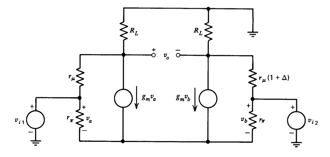
If the simplified transistor model used up to now were strictly valid, the \(\text{CMRR}\) for an amplifier with an emitter-circuit current source would be in finite regardless of whether a single-ended or a differential output is used, since the incremental resistance of the current source (which replaces \(R_E\) in Equation \(\ref{eq7.3.7}\)) is infinite. Analysis based on a more complete model shows that it is not possible to achieve infinite \(\text{CMRR}\) with a single-ended output, but that \(\text{CMRR}\) can be made arbitrarily high for a differential-output amplifier by matching all transistor parameters sufficiently closely. It is useful to illustrate the degradation that results from imperfect matching by example. Figure 7.8 shows a linear-region equivalent circuit for a differential amplifier. A collector-to-base resistance has been included in the transistor model.(We shall also see that an additional resistor between collector and emitter is necessary to complete the model. This second resistor is omitted from the present discussion since the simplified model illustrates the point adequately.) The physical reason for the presence of this element in the model is described in Section 8.3.1. The magnitude of this resistance is \(r_{\mu}\) for one transistor, while that of the second device differs by a fraction \(\Delta\). All other circuit parameters are identically matched. It is assumed that \(r_x\) is negligibly small compared to \(r_{\pi}\).(This assumption is frequently valid in the analysis of d-c amplifiers because the transistors are usually operated at low currents to decrease input current and to minimize offsets from differential self-heating. The resistance \(r_{\pi}\) grows approximately inversely with collector current, while the value of \(r_x\) is bounded, with a usual maximum value of 100 to 200 \(\Omega\). A typical value for \(r_{\pi}\) for transistors such as the 2N5963 is 2.5 M\(\Omega\) at an operating current of 10 \(\mu A\).) It is further assumed that the circuit has been constructed with an ideal emitter-circuit current source. Since \(r_{\mu} \gg R_L\), the gain for a differential input is
\[\dfrac{v_o}{(v_{i2} - v_{i1})}|_{v_{i1} = -v_{i2}} = g_m R_L\label{eq7.3.9} \]
The gain for a common-mode input is
\[\dfrac{v_o}{v_{i1}}|_{v_{i1} = v_{i2}} = \dfrac{\Delta R_{\mu} R_L}{(R_L + r_{\mu}) [(1 + \Delta ) r_{\mu} + R_L]} \nonumber \]
Again invoking the inequality \(r_{\mu} \gg R_L\) leads to
\[\dfrac{v_o}{v_{i1}}|_{v_{i1} = v_{i2}} \simeq \dfrac{\Delta R_L}{(1 + \Delta ) r_{\mu}}\label{eq7.3.11} \]
The resultant \(\text{CMRR}\) is obtained by dividing Equation \(\ref{eq7.3.9}\) by Equation \(\ref{eq7.3.11}\), yielding
\[\text{CMRR} = \dfrac{g_m (1 + \Delta ) r_{\mu}}{\Delta } \nonumber \]
A similar approach can be used to calculate common-mode errors that arise from other sources such as unequal transistor collector-to-emitter resistance or unequal values of \(r_x\). It can be shown that since each of these effects is small, there is little interaction among them, and it is valid to compute each error separately.
As a matter of practical interest, it is possible to obtain well enough matched transistors to obtain low-frequency values for \(\text{CMRR}\) on the order of \(10^4\) to \(10^6\) with a simple differential-amplifier connection.
Drift Attributable to Bipolar Transistors
The reason for the almost exclusive use of the differential amplifier for d-c amplifier circuits is because of the inherent drift cancellation afforded by symmetrical components. The purpose of this section is to indicate how the circuit should be balanced for minimum drift.
If a differential amplifier such as that shown in Figure 7.4 is constructed with symmetrical components, the differential output voltage \(v_{O1}\) is zero for \(v_{I1} = v_{I2}\). While resistors are available with virtually perfectly matched characteristics, selection of well-matched transistors is a significant problem.
It has been assumed up to this point that the transistors used in a differential amplifier are matched in the sense that they have equal saturation currents. One measure of the degree of match is to specify the ratio of the saturation currents for a pair of transistors. This ratio is exactly the same as the ratio of the collector currents of the two transistors when operated at equal base-to-emitter voltages, since at a base-to-emitter voltage \(V_{BE}\) (assuming operation at currents large compared to \(I_S\)), the collector current of one transistor is
\[I_{C1} = I_{S1} e^{qV_{BE}/kT} \nonumber \]
while that of the second transistor is
\[I_{C2} = I_{S2} e^{qV_{BE}/kT} \nonumber \]
Alternatively, the degree of match can be indicated by specifying the difference \(\Delta V\) between the base-to-emitter voltages of the two transistors when both are operated at some collector current \(I_C\). This specification implies that at some base-to-emitter voltage \(V_{BE}\)
\[I_{C1} = I_{S1} e^{qV_{BE}/kT} = I_C = I_{C2} = I_{S2} e^{q(V_{BE} + \Delta V)/kT}\label{eq7.3.15} \]
This measure of match is easily related to the degree of match between saturation currents, since Equation \(\ref{eq7.3.15}\) shows that
\[\dfrac{I_{S1}}{I_{S2}} = e^{q\Delta V/kT}\label{eq7.3.16} \]
Equation \(\ref{eq7.3.16}\) also shows that the base-to-emitter voltage mismatch, \(\Delta V\), is independent of the operating current level selected for the test.
If the circuit of Figure 7.4 is used as a d-c amplifier, the quantity \(\Delta V\) for the transistor pair is exactly the offset referred to the input of the amplifier, since this differential voltage must be applied to the input to equalize collector currents and thus make \(v_{O1}\) zero. For this reason, semiconductor manufacturers normally specify the degree of match between two transistors in terms of their base-to-emitter voltage differential at equal currents rather than as the ratio of saturation currents.
Several options are available to the designer to obtain well-matched pairs for use in differential amplifiers. Matched transistors are available from many manufacturers at a cost of from 2 to 10 times that of the two individual devices. These transistors are frequently mounted in a single can so that the differential temperature of the two chips is minimized. The best specified match available in a particular series of devices is typically a 3-mV base-to-emitter voltage differential when the devices operate at equal collector currents.
An alternative involves user matching of the transistors. This possibility is attractive for several reasons. There are economic advantages, particularly if large numbers of matched pairs are required, since relatively modest equipment suffices and since the effort required is not prohibitive. Better matches for a greater number of parameters are possible than with purchased matched pairs. However, lack of money, patience, and environmental control (remember the typical temperature coefficient of \(-2\ mV/ ^{\circ} C\)) generally limits achievable base-to-emitter voltage matches to the order of \(0.5\ mV\). It is also necessary to provide some sort of thermal coupling to keep the matched devices at equal temperatures during operation.
A third possibility is the use of a monolithic integrated-circuit differential pair. Through proper control of processing, all transistor parameters are simultaneously matched, and differential base-to-emitter voltages on the order of 1 mV are possible with present technology. Excellent thermal equality is obtained because of the proximity of the two devices. This approach is used as an integral part of all monolithic operational amplifiers. There are also a number of single and multiple monolithic matched pairs available for use in discrete designs. Several more sophisticated monolithic designs are available(Examples include the Fairchild Semiconductor \(\mu A726\) and \(\mu A727\)) that include temperature sensing and heating elements on the chip to keep its temperature relatively constant. The effects of ambient temperature variations are largely eliminated by this technique.
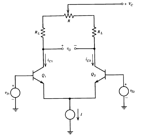
Regardless of the matching procedure used, some type of trimming is required to reduce the offset of the amplifier to zero at one temperature. One popular technique is to include a potentiometer in the emitter circuit as shown in Figure 7.9. The two bases are shorted together and the pot is adjusted until the two collector currents are equal so that \(v_O = 0\). This adjustment is possible for \(R > 2 \Delta V/I\), where \(\Delta V\) is the base-to-emitter voltage differential of the pair at equal collector currents. (The use of too large a potentiometer is undesirable since it lowers the transconductance(The transconductance of a differential pair is defined as the ratio of the incremental change in either collector current to the incremental differential input voltage. Assuming that both transistors have large values for \(\beta\) and negligible base resistance, the trans-conductance for the configuration shown in Figure 7.9 is \(\left |\dfrac{i_{c1}}{v_{i1} - v_{i2}} \right | = \left |\dfrac{i_{c2}}{v_{i1} - v_{i2}} \right | \simeq \dfrac{1}{1/g_{m1} + 1/g_{m2} + R} \)) of the pair, and we shall see that this quantity becomes important when the effect of other circuit components on drift is considered.) While this balance method is frequently used, it is fundamentally in error if minimization of drift with temperature is the design objective. The approach equalizes col lector currents and thus insures that one transistor operates at a quiescent base-to-emitter voltage of \(v_{BE1}\), while the other operates at a voltage of \(v_{BE1} + \Delta V\). The required difference in base-to-emitter voltages is obtained by adjusting the pot so that the voltages across its two segments differ by \(\Delta V\). Since the voltages across the pot segments are the same whenever the input voltage is adjusted to make vo zero (assuming the common-base cur rent gain of the transistors is one, the current through each pot segmen must be \(I/2\) when \(v_O = 0\)), the drift referred to the input with respect to
temperature for this design is identically equal to the differential change in the transistor base-to-emitter voltages with temperature. From Equation 7.2.5,
\[\dfrac{\partial}{\partial T} (v_{BE1} - v_{BE2})|_{i_{C1} = i_{C2} = \text{const}} = \left (\dfrac{v_{BE1} - V_{go}}{T} - \dfrac{3k}{q} \right ) - \left (\dfrac{v_{BE2} - V_{go}}{T} - \dfrac{3k}{q} \right ) = \dfrac{v_{BE1} - v{BE2}}{T} \nonumber \]
Since the difference \(v_{BE1} - v_{BE2}\) is \(\Delta V\),
\[\dfrac{\partial }{\partial T} (v_{BE1} - v_{BE2}) = \dfrac{\Delta V}{T} \nonumber \]
For example, a \(3-mV\) mismatch at room temperature leads to a drift of \(10\ \mu V/ ^{\circ} C\).
An alternative is to operate the transistors with equal base-to-emitter voltages. This condition requires that the quiescent collector-current ratio be equal to the ratio of the transistor saturation currents, or
\[\dfrac{I_{C1}}{I_{C2}} = \dfrac{I_{S1}}{I_{S2}} = e^{q\Delta V/kT} \nonumber \]
where, as defined above, (\Delta V\) is the difference between the base-to-emitter voltages of the two devices when they are operated at equal collector currents. In this case, a \(3-mV\) value for \(\Delta V\) requires a 12% difference in collector currents to equalize base-to-emitter voltages. A possible circuit configuration is shown in Figure 7.10. The two bases are shorted together, which forces equal base-to-emitter voltages and zero differential input voltage. The potentiometer is then adjusted to make \(v_O = 0\). The results of earlier analysis indicate that the temperature drift attributable to the transistors should be zero following this adjustment. While very low values are attainable by this method, there are other detailed effects, neglected in our simplified analysis, which lead to nonzero drift. It is possible to adjust the relative base-to-emitter voltages to compensate for these effects.(A. H. Hoffait and R. D. Thornton, "Limitations of Transistor DC Amplifiers," Proceedings Institute of Electrical and Electronic Engineers, February, 1964.) In practice, even the simplified balancing technique can result in drifts of a fraction of a microvolt per degree Centigrade.
It is stressed that this balancing technique should not be considered a substitute for careful matching of the devices, but rather as a final trim following matching. If a large base-to-emitter voltage mismatch is compensated for by this method, there is a large differential power dissipation with associated differential heating, base currents will differ by a large amount, and the transconductance of the pair will be significantly lower than if well-matched devices are used. For example, compensation for a \(60-mV\) mismatch requires collector currents with a 10 to 1 ratio and lowers trans-conductance by a factor of five compared with a well-matched pair operated at the same total emitter current. Operation with severely unbalanced collector currents also mismatches all current-dependent transistor parameters.
Other Drift Considerations
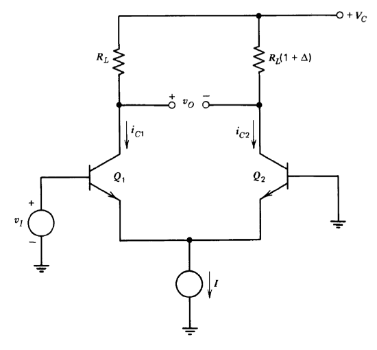
It is interesting to note that the excellent compensation afforded by even the simplified balancing technique described above emphasizes the drift contribution of other components in circuit. Consider the circuit shown in Figure 7.11. (For simplicity it is assumed that inputs are applied to only one side of the circuit.) Assume that the transistors are perfectly matched so that when the collector resistors are equal \(v_O = 0\) for \(v_I = 0\). A drift results if the relative collector-resistor values change as a result of differential changes with temperature or aging. The drift attributable to a collector-resistor fractional unbalance \(\Delta\) can be calculated as follows. With \(v_I = 0\), \(i_{C1} = i_{C2} \simeq I/2\). As \(v_i\) is increased, \(i_{C1} = I/2 + (g_m/2)v_i\) and \(i_{C2} = 1/2 - (g_m/2)v_i\), where \(g_m\) is the transconductance of either transistor. (It is assumed that \(r_{\pi} \gg r_x\) for the transistors.) In order to return \(v_O\) to zero, it is necessary to have
\[\left ( \dfrac{I}{2} + \dfrac{g_m}{2} v_i \right ) R_L = \left ( \dfrac{I}{2} - \dfrac{g_m}{2} v_i \right ) (1 + \Delta ) R_L \nonumber \]
or
\[g_m v_i = \dfrac{\Delta I}{2} \nonumber \]
(A term containing the small cross product \(g_mv_i \Delta R_L\) has been dropped.) Since each device is operating at a quiescent current level \(I/2\), \(g_m = qI/2kT \simeq 20I\) at room temperature. Thus the input voltage required to return the output voltage to zero (by definition the drift referred to the input) is \(\Delta /40\). The significance of this sensitivity is appreciated when one considers that two ordinary equal-value carbon-composition resistors can have temperature coefficients that differ by as much as one part per thousand per degree Centigrade. Use of such resistors would result in an amplifier drift of \(25 \mu V/ ^{\circ} C\)! It is clear that the quality of the resistors used is an important factor when a \(1 \mu V/ ^{\circ} C\) amplifier is designed.
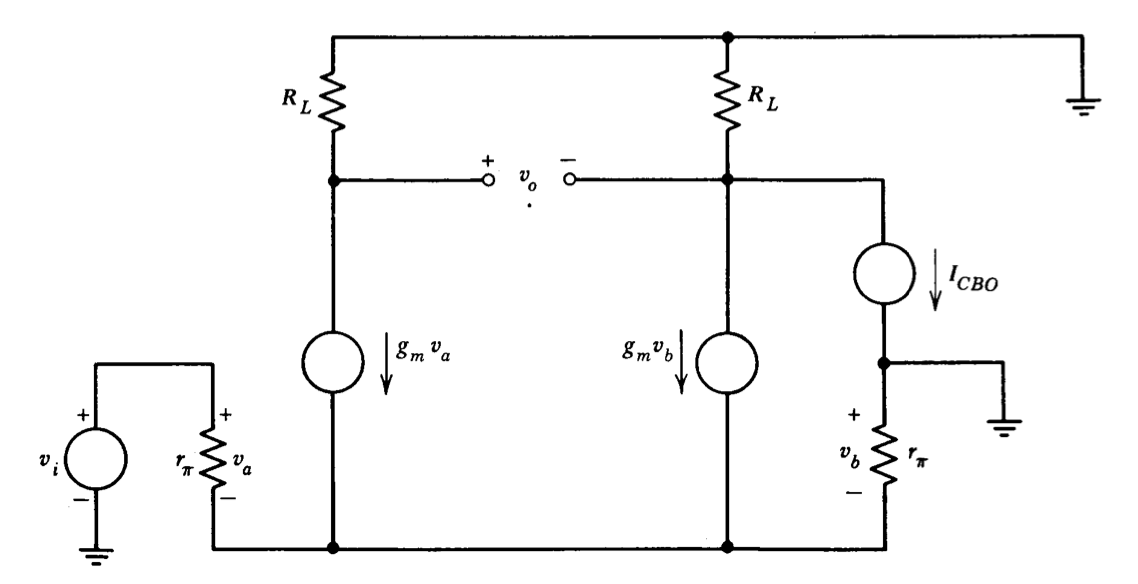
A similar conclusion is reached when the effects of collector-to-base leakage current \(I_{CBO}\)(The assumptions often used to simplify device physics to the contrary, this quantity is not related to the saturation current in the transistor equation. The magnitude of Is is dominated by effects within the body of the semiconductor, while the dominant component of \(I_{CBO}\), at least at room temperature, results from surface effects. Temperature coefficients are significantly different. While \(I_S\) doubles every \(6^{\circ} C\), \(I_{CBO}\) near room temperature typically doubles every \(10^{\circ} C\). ) are considered. An equivalent circuit that can be used to predict the drift from \(I_{CBO}\) is shown in Figure 7.12. Since the magnitude of \(I_{CBO}\) is likely to be significantly different for two otherwise well-matched transistors, only one leakage current generator is shown in Figure 7.12. Its value can be made the difference between the leakages if one component is not negligible. Proceeding as before, the value of \(v_i\) required to reduce the output to zero is given by solving
\[\dfrac{g_m v_i}{2} = \dfrac{-g_m v_i}{2} + I_{CBO} \nonumber \]
for \(v_i\), yielding
\[v_i = \dfrac{I_{CBO}}{g_m} \nonumber \]
The transconductance of either input transistor \(g_m\) can be related to the bias level for the differential pair (each member operates at 1/2) as \(g_m = 20I\). Therefore, the offset expressed in volts is \(I_{CBO}/20I\). Typical values are again evoked to illustrate the problem. The FT107A (an attractive choice for the input stage of a d-c amplifier since its specifications include a typical \(\beta\) of 1100 at \(10\mu A\) of collector current!) has a specified maximum leakage current that increases from essentially zero at \(25^{\circ} C\) to \(1 \mu A\) at \(125^{\circ} C\). The resultant average drift over the \(100^{\circ} C\) temperature range for the device operating at a collector current level of \(10 \mu A\) (\(I = 20 \mu A\)) is therefore bounded by \(25 \mu V/^{\circ} C\). Fortunately the typical value for \(I_{CBO}\) is 2 % of the maximum specified value, but additional screening procedures are required to insure this lower level is met by any particular device.
It is worth emphasizing the importance of proper thermal design for low-drift d-c amplifiers. A temperature differential of \(0.001^{\circ} C\) results in an offset of \(2 \mu V\) for a differential pair that is perfectly matched when the temperatures of the transistors are identical. Several factors influence the temperature differential of a pair. Good thermal contact between the members of the pair is mandatory. This required contact can be achieved by locating the two chips close together on a thermally conductive plate, or via monolithic integrated-circuit construction.
It is also necessary to minimize heating effects that disturb the pair. Self-heating as a consequence of the power dissipated in the pair is particularly important. Differential self-heating is reduced by operating the two members of the pair at matched, low collector currents and at low collector voltage. The location of other heat sources that can establish thermal gradients across the pair must also be considered. These sources are easily isolated in discrete-component designs, but impose severe constraints on component placement in integrated circuits.
Another aspect of the thermal problem involves the way in which the differential-amplifier transistors are connected to the input signal or to other circuit components. A thermocouple with an approximately \(20 \mu V/^{\circ} C\) coefficient is formed when kovar, an alloy frequently used for transistor leads, is connected to copper. Thus thermal gradients across the circuit, which result in different temperatures for series-connected thermocouple junctions in the signal path, can contribute significant offset voltage.