
7.6: CONCLUSIONS
- Page ID
- 69438
\( \newcommand{\vecs}[1]{\overset { \scriptstyle \rightharpoonup} {\mathbf{#1}} } \)
\( \newcommand{\vecd}[1]{\overset{-\!-\!\rightharpoonup}{\vphantom{a}\smash {#1}}} \)
\( \newcommand{\dsum}{\displaystyle\sum\limits} \)
\( \newcommand{\dint}{\displaystyle\int\limits} \)
\( \newcommand{\dlim}{\displaystyle\lim\limits} \)
\( \newcommand{\id}{\mathrm{id}}\) \( \newcommand{\Span}{\mathrm{span}}\)
( \newcommand{\kernel}{\mathrm{null}\,}\) \( \newcommand{\range}{\mathrm{range}\,}\)
\( \newcommand{\RealPart}{\mathrm{Re}}\) \( \newcommand{\ImaginaryPart}{\mathrm{Im}}\)
\( \newcommand{\Argument}{\mathrm{Arg}}\) \( \newcommand{\norm}[1]{\| #1 \|}\)
\( \newcommand{\inner}[2]{\langle #1, #2 \rangle}\)
\( \newcommand{\Span}{\mathrm{span}}\)
\( \newcommand{\id}{\mathrm{id}}\)
\( \newcommand{\Span}{\mathrm{span}}\)
\( \newcommand{\kernel}{\mathrm{null}\,}\)
\( \newcommand{\range}{\mathrm{range}\,}\)
\( \newcommand{\RealPart}{\mathrm{Re}}\)
\( \newcommand{\ImaginaryPart}{\mathrm{Im}}\)
\( \newcommand{\Argument}{\mathrm{Arg}}\)
\( \newcommand{\norm}[1]{\| #1 \|}\)
\( \newcommand{\inner}[2]{\langle #1, #2 \rangle}\)
\( \newcommand{\Span}{\mathrm{span}}\) \( \newcommand{\AA}{\unicode[.8,0]{x212B}}\)
\( \newcommand{\vectorA}[1]{\vec{#1}} % arrow\)
\( \newcommand{\vectorAt}[1]{\vec{\text{#1}}} % arrow\)
\( \newcommand{\vectorB}[1]{\overset { \scriptstyle \rightharpoonup} {\mathbf{#1}} } \)
\( \newcommand{\vectorC}[1]{\textbf{#1}} \)
\( \newcommand{\vectorD}[1]{\overrightarrow{#1}} \)
\( \newcommand{\vectorDt}[1]{\overrightarrow{\text{#1}}} \)
\( \newcommand{\vectE}[1]{\overset{-\!-\!\rightharpoonup}{\vphantom{a}\smash{\mathbf {#1}}}} \)
\( \newcommand{\vecs}[1]{\overset { \scriptstyle \rightharpoonup} {\mathbf{#1}} } \)
\( \newcommand{\vecd}[1]{\overset{-\!-\!\rightharpoonup}{\vphantom{a}\smash {#1}}} \)
\(\newcommand{\avec}{\mathbf a}\) \(\newcommand{\bvec}{\mathbf b}\) \(\newcommand{\cvec}{\mathbf c}\) \(\newcommand{\dvec}{\mathbf d}\) \(\newcommand{\dtil}{\widetilde{\mathbf d}}\) \(\newcommand{\evec}{\mathbf e}\) \(\newcommand{\fvec}{\mathbf f}\) \(\newcommand{\nvec}{\mathbf n}\) \(\newcommand{\pvec}{\mathbf p}\) \(\newcommand{\qvec}{\mathbf q}\) \(\newcommand{\svec}{\mathbf s}\) \(\newcommand{\tvec}{\mathbf t}\) \(\newcommand{\uvec}{\mathbf u}\) \(\newcommand{\vvec}{\mathbf v}\) \(\newcommand{\wvec}{\mathbf w}\) \(\newcommand{\xvec}{\mathbf x}\) \(\newcommand{\yvec}{\mathbf y}\) \(\newcommand{\zvec}{\mathbf z}\) \(\newcommand{\rvec}{\mathbf r}\) \(\newcommand{\mvec}{\mathbf m}\) \(\newcommand{\zerovec}{\mathbf 0}\) \(\newcommand{\onevec}{\mathbf 1}\) \(\newcommand{\real}{\mathbb R}\) \(\newcommand{\twovec}[2]{\left[\begin{array}{r}#1 \\ #2 \end{array}\right]}\) \(\newcommand{\ctwovec}[2]{\left[\begin{array}{c}#1 \\ #2 \end{array}\right]}\) \(\newcommand{\threevec}[3]{\left[\begin{array}{r}#1 \\ #2 \\ #3 \end{array}\right]}\) \(\newcommand{\cthreevec}[3]{\left[\begin{array}{c}#1 \\ #2 \\ #3 \end{array}\right]}\) \(\newcommand{\fourvec}[4]{\left[\begin{array}{r}#1 \\ #2 \\ #3 \\ #4 \end{array}\right]}\) \(\newcommand{\cfourvec}[4]{\left[\begin{array}{c}#1 \\ #2 \\ #3 \\ #4 \end{array}\right]}\) \(\newcommand{\fivevec}[5]{\left[\begin{array}{r}#1 \\ #2 \\ #3 \\ #4 \\ #5 \\ \end{array}\right]}\) \(\newcommand{\cfivevec}[5]{\left[\begin{array}{c}#1 \\ #2 \\ #3 \\ #4 \\ #5 \\ \end{array}\right]}\) \(\newcommand{\mattwo}[4]{\left[\begin{array}{rr}#1 \amp #2 \\ #3 \amp #4 \\ \end{array}\right]}\) \(\newcommand{\laspan}[1]{\text{Span}\{#1\}}\) \(\newcommand{\bcal}{\cal B}\) \(\newcommand{\ccal}{\cal C}\) \(\newcommand{\scal}{\cal S}\) \(\newcommand{\wcal}{\cal W}\) \(\newcommand{\ecal}{\cal E}\) \(\newcommand{\coords}[2]{\left\{#1\right\}_{#2}}\) \(\newcommand{\gray}[1]{\color{gray}{#1}}\) \(\newcommand{\lgray}[1]{\color{lightgray}{#1}}\) \(\newcommand{\rank}{\operatorname{rank}}\) \(\newcommand{\row}{\text{Row}}\) \(\newcommand{\col}{\text{Col}}\) \(\renewcommand{\row}{\text{Row}}\) \(\newcommand{\nul}{\text{Nul}}\) \(\newcommand{\var}{\text{Var}}\) \(\newcommand{\corr}{\text{corr}}\) \(\newcommand{\len}[1]{\left|#1\right|}\) \(\newcommand{\bbar}{\overline{\bvec}}\) \(\newcommand{\bhat}{\widehat{\bvec}}\) \(\newcommand{\bperp}{\bvec^\perp}\) \(\newcommand{\xhat}{\widehat{\xvec}}\) \(\newcommand{\vhat}{\widehat{\vvec}}\) \(\newcommand{\uhat}{\widehat{\uvec}}\) \(\newcommand{\what}{\widehat{\wvec}}\) \(\newcommand{\Sighat}{\widehat{\Sigma}}\) \(\newcommand{\lt}{<}\) \(\newcommand{\gt}{>}\) \(\newcommand{\amp}{&}\) \(\definecolor{fillinmathshade}{gray}{0.9}\)The successful design of low-drift direct-coupled amplifiers depends on exploiting the unique tracking properties of the differential amplifier, and the application of a number of drift reducing tricks that have evolved. In view of the many possible pitfalls, it is reassuring to realize that the drift of several commercially available integrated-circuit operational amplifiers is on the order of 3 \(\mu V\) per degree Centigrade or lower, and that at least one discrete-component design achieves a drift of 0.5 \(\mu V\) per degree Centi grade.
The purpose of the simple but somewhat tedious derivations and examples of this section has not been to permit exact evaluation of the drift of a circuit, but rather to emphasize that "little things mean a lot," and to indicate the dominant drift sources of a particular design so that they may be reduced.
PROBLEMS
Exercise \(\PageIndex{1}\)
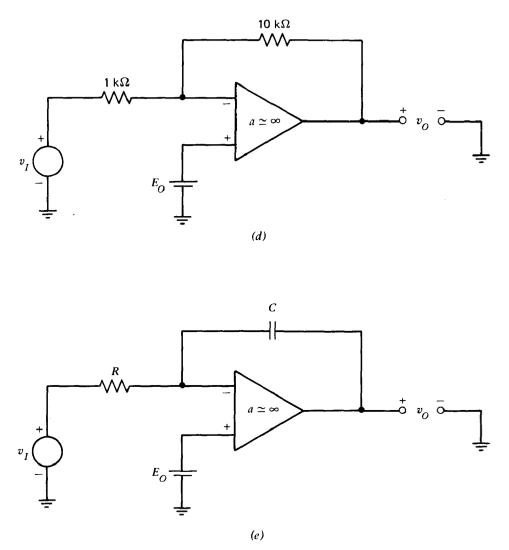
Figure 7.23 shows several amplifying connections that consist of ideal amplifiers and passive components. Offset sources are shown as batteries. Calculate the offset referred to the input (the input voltage required to make \(v_O = 0\)), the output offset (the output voltage with \(v_I = 0\)), and the gain \((v_o /v_i)\) for each connection.
Exercise \(\PageIndex{2}\)
Consider an operational amplifier with a particular value of offset \(E_O\) referred to its input. Compare the offset referred to the input of amplifier connections that combine this amplifier with passive components to pro vide inverting or noninverting gains with a magnitude of \(A\).
Exercise \(\PageIndex{3}\)
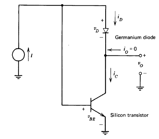
Figure 7.24 shows a circuit that can provide a temperature-independent output voltage. Assume that the transistor has very high \(\beta\) and that \(i_O = 0\). The diode variables are related as
\[i_D = A_d T^3 e^{q(v_D - 0.782)/kT} \nonumber \]
while the transistor relationship is
\[i_C = A_t T^3 e^{q(v_{BE} - 1.205)/kT} \nonumber \]
(a) For what ratio of \(A_d\) to \(A_t\) does \(\partial v_O/\partial T = 0\)?
(b) What is \(v_O\) with the condition of part \(a\) satisfied?
(c) What is the output resistance of this connection?
Exercise \(\PageIndex{4}\)
The current-voltage relationship for a family of diodes can be approxi mated as
\[i_D = K e^{q(v_D - 1.2)/kT}\nonumber \]
where \(K\) is a (temperature-independent) constant that may vary from diode to diode.
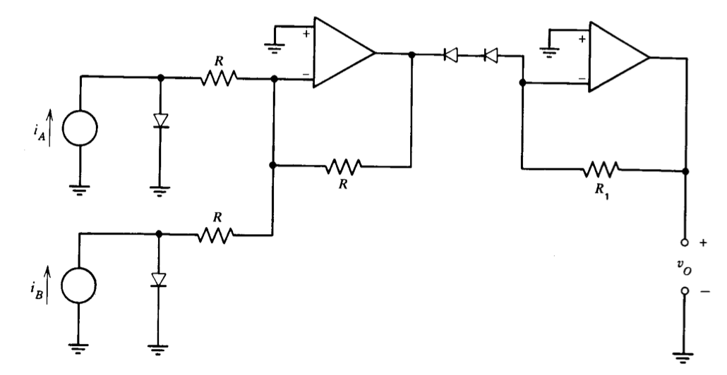
(a) Four of these diodes with identical values for \(K\) are connected as shown in Figure 7.25. Find \(v_O\) as a function if \(i_A\) and \(i_B\). You may assume that the currents through all resistors \(R\) are much smaller than \(i_A\) or \(i_B\) and that both operational amplifiers are ideal.
(b) Determine an expression for
\[\dfrac{\partial v_D}{\partial T} |_{i_D = \text{const}} \text{ for these diodes.}\nonumber \]
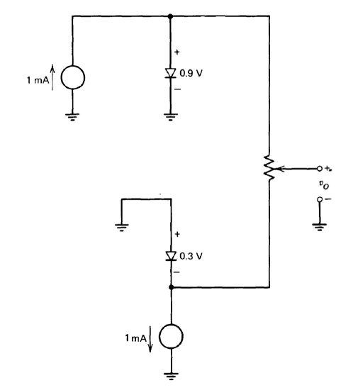
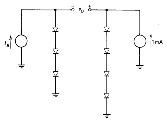
(c) Assume that, because of incredibly poor control of the process used to make these diodes, it is possible to find two diodes which, at \(T = 300^{\circ} K\) and \(1\ mA\) of forward current, have forward voltages of 0.3 \(V\) and 0.9 \(V\), respectively. These diodes are connected as shown in Figure 7.26, and the pot is adjusted so that \(\partial v_O/\partial T = 0\). What is vo with this pot setting?
Exercise \(\PageIndex{5}\)
The current-voltage relationship for a particular diode is
\[i_D = AT^{2.5} e^{q(v_D - 1.205)/kT}\nonumber \]
The value of the constant \(A\) is such that at \(300^{\circ} K\) and \(v_D = 0.6\ V\), \(i_D = 1\ mA\).
(a) Determine \(\dfrac{\partial v_D}{\partial T} |_{i_D = \text{const}}\)
(b) Seven identical diodes are connected as shown in Figure 7.27. By appropriate choice of \(i_B\), it is possible to make vo temperature independent over a limited range of temperature. Determine the required value of \(v_O\) so that
\[\dfrac{\partial v_O}{\partial T} |_{i_B = \text{const}} = 0 \ \ \ \text{ at } T = 300^{\circ} K\nonumber \]
Approximate the value of \(I_B\) necessary to obtain the required value of \(v_O\).
(c) Calculate the second derivative of vo with respect to temperature. Use this value to estimate the temperature range over which \(v_O\) remains within one part in \(10^5\) of its \(300^{\circ} K\) value.
(d) Repeat part \(b\) assuming that the magnitude of the right-hand current source is increased to \(10\ mA\).
The type of voltage reference that results from this topology is called a band-gap reference. The underlying principle is used as a voltage reference in several available integrated circuits.
Exercise \(\PageIndex{6}\)
A differential amplifier is built with the topology shown in Figure 7.11, with the exception that signals may also be applied to the base of the right-hand transistor. The value of the current source is 20 \(\mu A\), and the incre mental output resistance of this element is 10 \(M\Omega\). (The reasons for finite output resistance from current sources are discussed in Section 8.3.5.) Cal culate the common-mode rejection ratio of this amplifier as a function the fractional unbalance in collector load resistors, \(\Delta\), assuming all transistor parameters are perfectly matched.
Exercise \(\PageIndex{7}\)
An operational amplifier is built using a bipolar-transistor differential input stage. It is found that when the inverting input of the amplifier is grounded, the output voltage of the amplifier is zero at \(25^{\circ} C\) when a positive voltage of magnitude \(\Delta V\) is applied to the noninverting input of the amplifier. You may assume that this offset and any temperature-dependent drift of the operational amplifier are caused only by a mismatch between the quantities \(I_S\) of the input-transistor pair, and that transistor variables are related by Equation 7.2.1.
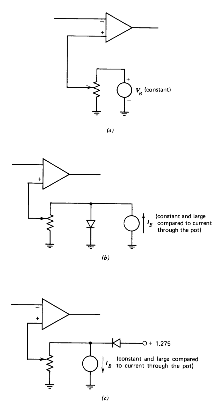
The operational amplifier is intended for use in an inverting-amplifier connection, and therefore it is possible to reduce the effective offset at the inverting input to zero at \(25^{\circ} C\) by applying a voltage \(\Delta V\) to the noninverting input. Three techniques for obtaining this bias voltage are indicated in Figure 7.28. Comment on the effectiveness of these three balancing methods in reducing the temperature drift of the amplifier. Assume that the diode
forward-voltage variation with temperature is given by
\[\dfrac{\partial v_D}{\partial T} |_{i_D = \text{const}} = \dfrac{(v_D - V_{go})}{T} - \dfrac{3k}{q}\nonumber \]
in parts \(b\) and \(c\).
Exercise \(\PageIndex{8}\)
A differential amplifier is constructed and balanced as shown in Figure 7.10. Following balancing, it is found that transistor \(Q_1\) is operating at a quiescent collector current of \(1.1\ mA\), while \(Q_2\) operates at a collector cur rent of \(0.9\ mA\). The transistors used are discrete devices mounted in reasonably close thermal proximity, and have a differential thermal resistance of \(20^{\circ} C\) per watt (i.e., if one member of the pair operates at a power level \(\Delta P\) watts above that of the other, its temperature is \(20 \times \Delta P\) degrees Centigrade higher). Estimate the offset referred to the input that results for a one-volt change in power-supply voltage.
Exercise \(\PageIndex{9}\)
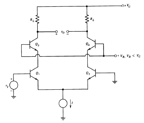
A differential amplifier that can provide low input capacitance, and, by proper control of bias voltage \(V_B\), high common-mode rejection ratio, is shown in Figure 7.29. Assume that \(Q_1\) and \(Q_2\) are perfectly matched. Further assume that \(\beta_3 = \beta_4 = 100\) at \(25^{\circ} C\). The output voltage is then zero for \(v_I = 0\). Assume that the fractional change in \(\beta_3\) is 0.5 % per degree Centi grade, while that of \(\beta_4\) is 1% per degree Centigrade. Calculate the offset referred to the input for a \(1^{\circ} C\) temperature change.
Exercise \(\PageIndex{10}\)
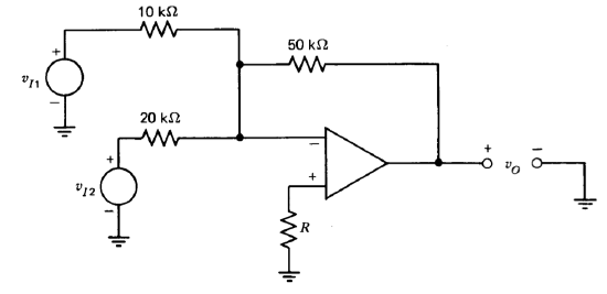
An operational amplifier is found to have a bias-current requirement at its noninverting input that is 10% higher than that at its inverting input at all temperatures of interest. The amplifier is connected as shown in Figure 7.30. Select the value of \(R\) that minimizes the effect of input current on circuit performance.
Exercise \(\PageIndex{11}\)
The current at the inverting input of a certain operational amplifier is found to be equal to \(10^{-3}A/T^2\) where \(T\) is the temperature in degrees Kelvin. The amplifier is to be used in an inverting connection; consequently the technique illustrated in Figure 7.15 can be employed for input-current compensation. Parameters are selected so that the diode operates at a very nearly constant \(1\ mA\), and its forward voltage at \(300^{\circ} K\) is \(600\ mV\) at this current. The diode current-voltage characteristics are of the general form
\[i_D = AT^3 e^{q(V_D - C_{go})/kT}\nonumber \]
Select resistor \(R_2\) and bias source \(V_A\) in Figure 7.15 so that the input current and its derivative with respect to temperature are cancelled at \(300^{\circ} K\). What is the maximum compensated input current over the temperature range of 250 to \(350^{\circ} K\) using this form of compensation? Contrast this range with the corresponding quantity obtained with no compensation and by cancelling the input current at \(300^{\circ} K\) with a fixed bias current.
Exercise \(\PageIndex{12}\)
The use of Darlington-connected input-stage transistors is discussed in Section 7.4.4. An alternative high-gain connection is the complementary Darlington connection shown in Figure 7.31\(a\). A differential amplifier employing this connection is shown in Figure 7.31\(b\). Determine the voltage drift of this connection as a function of relative current-gain changes of the \(Q_1-Q_2\) pair by an argument similar to that used for Figure 7.20.
Exercise \(\PageIndex{13}\)
A regulated power supply is constructed as shown in Figure 7.32. This supply uses feedback around a very simple d-c amplifier in an attempt to make \(v_O = V_R\).
(a) Determine the output voltage for circuit values as shown.
(b) How much does the output voltage change for a small fractional change in the current gain of \(Q_2\)?
(c) Suggest a circuit modification that will reduce the dependence of \(v_O\) on the fractional change in \(\beta_2\).