
10.2: FABRICATION
- Page ID
- 58470
\( \newcommand{\vecs}[1]{\overset { \scriptstyle \rightharpoonup} {\mathbf{#1}} } \)
\( \newcommand{\vecd}[1]{\overset{-\!-\!\rightharpoonup}{\vphantom{a}\smash {#1}}} \)
\( \newcommand{\dsum}{\displaystyle\sum\limits} \)
\( \newcommand{\dint}{\displaystyle\int\limits} \)
\( \newcommand{\dlim}{\displaystyle\lim\limits} \)
\( \newcommand{\id}{\mathrm{id}}\) \( \newcommand{\Span}{\mathrm{span}}\)
( \newcommand{\kernel}{\mathrm{null}\,}\) \( \newcommand{\range}{\mathrm{range}\,}\)
\( \newcommand{\RealPart}{\mathrm{Re}}\) \( \newcommand{\ImaginaryPart}{\mathrm{Im}}\)
\( \newcommand{\Argument}{\mathrm{Arg}}\) \( \newcommand{\norm}[1]{\| #1 \|}\)
\( \newcommand{\inner}[2]{\langle #1, #2 \rangle}\)
\( \newcommand{\Span}{\mathrm{span}}\)
\( \newcommand{\id}{\mathrm{id}}\)
\( \newcommand{\Span}{\mathrm{span}}\)
\( \newcommand{\kernel}{\mathrm{null}\,}\)
\( \newcommand{\range}{\mathrm{range}\,}\)
\( \newcommand{\RealPart}{\mathrm{Re}}\)
\( \newcommand{\ImaginaryPart}{\mathrm{Im}}\)
\( \newcommand{\Argument}{\mathrm{Arg}}\)
\( \newcommand{\norm}[1]{\| #1 \|}\)
\( \newcommand{\inner}[2]{\langle #1, #2 \rangle}\)
\( \newcommand{\Span}{\mathrm{span}}\) \( \newcommand{\AA}{\unicode[.8,0]{x212B}}\)
\( \newcommand{\vectorA}[1]{\vec{#1}} % arrow\)
\( \newcommand{\vectorAt}[1]{\vec{\text{#1}}} % arrow\)
\( \newcommand{\vectorB}[1]{\overset { \scriptstyle \rightharpoonup} {\mathbf{#1}} } \)
\( \newcommand{\vectorC}[1]{\textbf{#1}} \)
\( \newcommand{\vectorD}[1]{\overrightarrow{#1}} \)
\( \newcommand{\vectorDt}[1]{\overrightarrow{\text{#1}}} \)
\( \newcommand{\vectE}[1]{\overset{-\!-\!\rightharpoonup}{\vphantom{a}\smash{\mathbf {#1}}}} \)
\( \newcommand{\vecs}[1]{\overset { \scriptstyle \rightharpoonup} {\mathbf{#1}} } \)
\(\newcommand{\longvect}{\overrightarrow}\)
\( \newcommand{\vecd}[1]{\overset{-\!-\!\rightharpoonup}{\vphantom{a}\smash {#1}}} \)
\(\newcommand{\avec}{\mathbf a}\) \(\newcommand{\bvec}{\mathbf b}\) \(\newcommand{\cvec}{\mathbf c}\) \(\newcommand{\dvec}{\mathbf d}\) \(\newcommand{\dtil}{\widetilde{\mathbf d}}\) \(\newcommand{\evec}{\mathbf e}\) \(\newcommand{\fvec}{\mathbf f}\) \(\newcommand{\nvec}{\mathbf n}\) \(\newcommand{\pvec}{\mathbf p}\) \(\newcommand{\qvec}{\mathbf q}\) \(\newcommand{\svec}{\mathbf s}\) \(\newcommand{\tvec}{\mathbf t}\) \(\newcommand{\uvec}{\mathbf u}\) \(\newcommand{\vvec}{\mathbf v}\) \(\newcommand{\wvec}{\mathbf w}\) \(\newcommand{\xvec}{\mathbf x}\) \(\newcommand{\yvec}{\mathbf y}\) \(\newcommand{\zvec}{\mathbf z}\) \(\newcommand{\rvec}{\mathbf r}\) \(\newcommand{\mvec}{\mathbf m}\) \(\newcommand{\zerovec}{\mathbf 0}\) \(\newcommand{\onevec}{\mathbf 1}\) \(\newcommand{\real}{\mathbb R}\) \(\newcommand{\twovec}[2]{\left[\begin{array}{r}#1 \\ #2 \end{array}\right]}\) \(\newcommand{\ctwovec}[2]{\left[\begin{array}{c}#1 \\ #2 \end{array}\right]}\) \(\newcommand{\threevec}[3]{\left[\begin{array}{r}#1 \\ #2 \\ #3 \end{array}\right]}\) \(\newcommand{\cthreevec}[3]{\left[\begin{array}{c}#1 \\ #2 \\ #3 \end{array}\right]}\) \(\newcommand{\fourvec}[4]{\left[\begin{array}{r}#1 \\ #2 \\ #3 \\ #4 \end{array}\right]}\) \(\newcommand{\cfourvec}[4]{\left[\begin{array}{c}#1 \\ #2 \\ #3 \\ #4 \end{array}\right]}\) \(\newcommand{\fivevec}[5]{\left[\begin{array}{r}#1 \\ #2 \\ #3 \\ #4 \\ #5 \\ \end{array}\right]}\) \(\newcommand{\cfivevec}[5]{\left[\begin{array}{c}#1 \\ #2 \\ #3 \\ #4 \\ #5 \\ \end{array}\right]}\) \(\newcommand{\mattwo}[4]{\left[\begin{array}{rr}#1 \amp #2 \\ #3 \amp #4 \\ \end{array}\right]}\) \(\newcommand{\laspan}[1]{\text{Span}\{#1\}}\) \(\newcommand{\bcal}{\cal B}\) \(\newcommand{\ccal}{\cal C}\) \(\newcommand{\scal}{\cal S}\) \(\newcommand{\wcal}{\cal W}\) \(\newcommand{\ecal}{\cal E}\) \(\newcommand{\coords}[2]{\left\{#1\right\}_{#2}}\) \(\newcommand{\gray}[1]{\color{gray}{#1}}\) \(\newcommand{\lgray}[1]{\color{lightgray}{#1}}\) \(\newcommand{\rank}{\operatorname{rank}}\) \(\newcommand{\row}{\text{Row}}\) \(\newcommand{\col}{\text{Col}}\) \(\renewcommand{\row}{\text{Row}}\) \(\newcommand{\nul}{\text{Nul}}\) \(\newcommand{\var}{\text{Var}}\) \(\newcommand{\corr}{\text{corr}}\) \(\newcommand{\len}[1]{\left|#1\right|}\) \(\newcommand{\bbar}{\overline{\bvec}}\) \(\newcommand{\bhat}{\widehat{\bvec}}\) \(\newcommand{\bperp}{\bvec^\perp}\) \(\newcommand{\xhat}{\widehat{\xvec}}\) \(\newcommand{\vhat}{\widehat{\vvec}}\) \(\newcommand{\uhat}{\widehat{\uvec}}\) \(\newcommand{\what}{\widehat{\wvec}}\) \(\newcommand{\Sighat}{\widehat{\Sigma}}\) \(\newcommand{\lt}{<}\) \(\newcommand{\gt}{>}\) \(\newcommand{\amp}{&}\) \(\definecolor{fillinmathshade}{gray}{0.9}\)The process used to make monolithic integrated circuits dictates the type and performance of components that can be realized. Since the probabilities of success of each step of the fabrication process multiply to yield the probability of successfully completing a circuit, manufacturers are understandably reluctant to introduce additional operations that must reduce yields and thereby increase the cost of the final circuit. Some manufacturers do use processes that are more involved than the one described here and thus increase the variety and quality of the components they can form, but unfortunately the circuits made by these more complex processes can usually be easily recognized by their higher costs.
The most common process used to manufacture both linear and digital integrated circuits is the six-mask planar-epitaxial process. This technology evolved from that used to make planar transistors. Each masking operation itself involves a number of steps, the more important of which are as follows. A silicon-dioxide layer is first formed by exposing the silicon integrated-circuit material to steam or oxygen at elevated temperatures. This layer is photosensitized, and regions are defined by photographically exposing the wafer using a specific pattern, developing the resultant image, and removing unhardened photosensitive material to expose the oxide layer. This layer is then etched away in the unprotected regions. The oxide layer itself thus forms a mask which permits \(N\)- or \(P\)-type dopants to be diffused into the silicon wafer. Following diffusion, the oxide is reformed and the masking process repeated to define new areas.
While the operation described above seems complex, particularly when we consider that it is repeated six times, a large number of complete circuits can be fabricated simultaneously. The circuits can be tested individually so localized defects can be eliminated. The net result is that a large number of functioning circuits are obtained from each successfully processed silicon wafer at a low average cost per circuit.
Transistors
The six-mask process is tailored for making NPN transistors, and transistors with characteristics similar to those of virtually all discrete types can be formed by the process. The other components necessary to complete the circuit must be made during the same operations that form the NPN transistors.
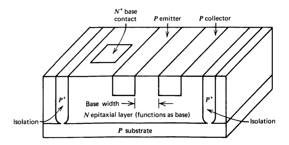
A cross-sectional view of an NPN transistor made by the six-mask planar-epitaxial process is shown in Figure 10.1.(It is cautioned that in this and following figures, relative dimensions have been grossly distorted in order to present clearly essential features. In particular, vertical dimensions in the epitaxial layer have been expanded relative to other dimensions. The minimum horizontal dimension is constrained to the order of 0.001 inch by uncertainties associated with the photographic definition of adjacent regions. Conversely, vertical dimensions in the epitaxial layer are defined by diffusion depths and are typically a factor of 10 to 100 times smaller.) Fabrication starts with a \(P\)-type
substrate (relatively much thicker than that shown in the figure) that provides mechanical rigidity to the entire structure. The first masking operation is used to define heavily doped \(N\)-type (designated as \(N^+\)) regions in the substrate. The reason for these subcollector or buried-layer regions will be described subsequently. A relatively lightly doped \(N\) layer that will be the collector of the complete transistor is then formed on top of the substrate by a process of epitaxial growth.
The next masking operation performed on the epitaxial layer creates heavily doped \(P\)-type (or \(P^+\)) regions that extend completely through the epitaxial layer to the substrate. These isolation regions in conjunction with the substrate separate the epitaxial layer into a number of N regions each surrounded by P material. The substrate (and thus the isolation regions) will be connected to the most negative voltage applied to the circuit. Since the \(N\) regions adjacent to the isolation and substrate cannot be negatively biased with respect to these regions, the various \(N\) regions are electrically isolated from each other by reverse-biased \(P-N\) junctions. Subsequent steps in the process will convert each isolated area into a separate component.
The \(P\)-type base region is formed during the next masking operation. The transistor is completed by diffusing an \(N^+\) emitter into the base. A collector contact, the need for which is described below, is formed in the collector region during the emitter diffusion. The oxide layer is regrown for the last time, and windows that will allow contact to the various regions are etched into this oxide. The entire wafer is then exposed to vaporized aluminum, which forms a thin aluminum layer over the surface. The final masking operation separates this aluminum layer into the conductor pattern that interconnects the various components.
The six masking operations described above can be summarized as follows:
- Subcollector or buried layer
- Isolation
- Base
- Emitter
- Contact window
- Conductor pattern
The buried layer and the heavily doped collector-contact regions are included for the following reasons. Recall that in order to reduce reverse injection from the base of a transistor into its emitter which lowers current gain, it is necessary to have the relative doping level of the emitter significantly greater than that of the base. It is also necessary to dope the collector lightly with respect to the base so that the collector space-charge layer extends dominantly into the collector region in order to prevent low collector-to-base breakdown voltage. As a result of these cascaded inequalities, the collector region is quite lightly doped and thus has high resistivity. If collec tor current had to flow laterally through this high-resistivity material, a transistor would have a large resistor in series with its collector. The low-resistivity subcollector acts as a shorting bar that connects the active collector region immediately under the base to the collector contact. The length of the collector current path through the high resistivity region is shortened significantly by the subcollector. (Remember that the vertical dimensions in the epitaxial region are actually much shorter than horizontal dimensions.)
The heavily doped \(N^+\) collector contact is necessary to prevent the collector material from being converted to P type by the aluminum that is a \(P\)-type dopant. It is interesting to note that the Schottky-diode junction that can form when aluminum is deposited on lightly doped \(N\) material is used as a clamp diode in certain digital integrated circuits.
As mentioned earlier, excellent NPN transistors can be made by this process, and the performance of certain designs can be better than that of their discrete-component counterparts. For example, the collector-to-base capacitance of modern high-speed transistors can be dominated by lead rather than space-charge-layer capacitance. The small geometries possible with integrated circuits reduce interconnection capacitance. Furthermore, NPN transistors are extremely economical to fabricate by this method, with the incremental increase in selling price attributable to adding one transistor to a circuit being a fraction of a cent.
Since all transistors on a particular wafer are formed simultaneously, all must have similar characteristics (to within the uniformity of the processing) on a per-unit-area basis. This uniformity is in fact often exploited for the fabrication of matched transistors. A degree of design freedom is retained through adjustment of the relative active areas of various transistors in a circuit, since the collector current of a transistor at fixed base-to-emitter voltage is proportional to its area. This relationship is frequently used to control the collector-current ratios of several transistors (see Section 10.3). Alternatively, the area of a transistor may be selected to optimize current gain at its anticipated quiescent current level. Thus transistors used in the output stage of an operational amplifier are frequently larger than those used in its input stage.
A recent innovation(R. J. Widlar, "Super Gain Transistors for IC's," National Semiconductor Corporation, Technical Paper TP-1 1, March, 1969. ) used in some high-performance designs incorporates two emitter diffusions to significantly increase the current gain of certain transistors in the circuit. The oxide layer is first etched away in the emitter
region of selected transistors, and the first emitter diffusion is completed. Then, without any oxide regrowth, the emitter regions of the remaining transistors are exposed and the second emitter diffusion is completed. The transistors that have received both emitter diffusions are sometimes called "super-\(\beta\)" transistors since the narrow base width that results from the two diffusions can yield current gains between \(10^3\) and \(10^4\). The narrow base region also lowers collector-to-base breakdown voltage to several volts, and precautions must be taken in circuits that use these devices to insure that the breakdown voltage is not exceeded. A second problem is that an overzealous diffusion schedule can easily reduce the base width to zero, and the price of amplifiers using super-\(\beta\) transistors usually reflects this possibility.
Transistors
The six-mask epitaxial process normally used for monolithic integrated circuits is optimized for the fabrication of NPN transistors, and any other circuit components are compromised in that they must be made compatible with the NPN fabrication. One of the limitations of the process is that high-quality PNP transistors cannot be made by it. This limitation is particularly severe in view of the topological advantages associated with the use of complementary transistors. For example, the voltage level shifting required to make input and output voltage ranges overlap in an operational amplifier is most easily accomplished by using one polarity device for the input stage combined with the complementary type in the second stage. Similarly, designs for output stages that do not require high quiescent current are cumbersome unless complementary devices are used.
One type PNP transistor that can be made by the six-mask process is called a lateral PNP. This device is made using the NPN base diffusion for both the emitter and collector regions. The N-type epitaxial layer is used as the base region. Figure 10.2 shows a cross-sectional view of one possible geometry.(Practical geometries usually surround the emitter stripe with a collector region. This refinement does not alter the basic operation of the device.) Current flows laterally from emitter to collector in this structure, in contrast to the vertical flow that results in a conventional design.
There are a number of problems associated with the lateral PNP transistor. The relative doping levels of its emitter, base, and collector regions are far from optimum. More important, however, is the fact that the base width for the structure is controlled by a masking operation rather than a diffusion depth, and is one to two orders of magnitude greater than that of a conventional transistor. There is also parasitic current gain to the substrate that acts as a second collector for the transistor. These effects originally combined to produce very low current gain, with values for \(\beta\) of less than unity common in early lateral PNP'S. More recently, process refinements primarily involving the use of the buried layer to reduce parasitic current gain have resulted in current gains in excess of 100.
A more fundamental limitation is that the extremely wide base leads to excessive charge storage in this region and consequently very low values for fT. The phase shift associated with this configuration normally limits to 1 to 2 MHz the closed-loop bandwidth of an operational amplifier that includes a lateral PNP in the gain path.
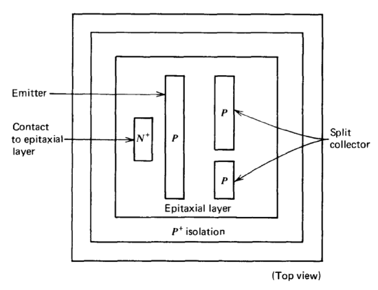
One interesting variation of the lateral-PNP transistor is shown in Figure10.3. The base-to-emitter voltage applied to this device establishes the per unit-length current density that flows in a direction perpendicular to the emitter. The relative currents intercepted by the two collectors are thus equal to the relative collector lengths. The concept can be extended, and lateral-PNP transistors with three or more collectors are used in some designs.
One advantage of the lateral-PNP structure is that the base-to-emitter breakdown voltage of this device is equal to the collector-to-base breakdown voltage of the NPN transistors that are formed by the same process. This feature permits nonlinear operation with large different input voltages for operational amplifiers that include lateral PNP's in their input stage. (Two examples are given in Section 10.4.)
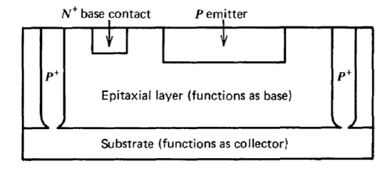
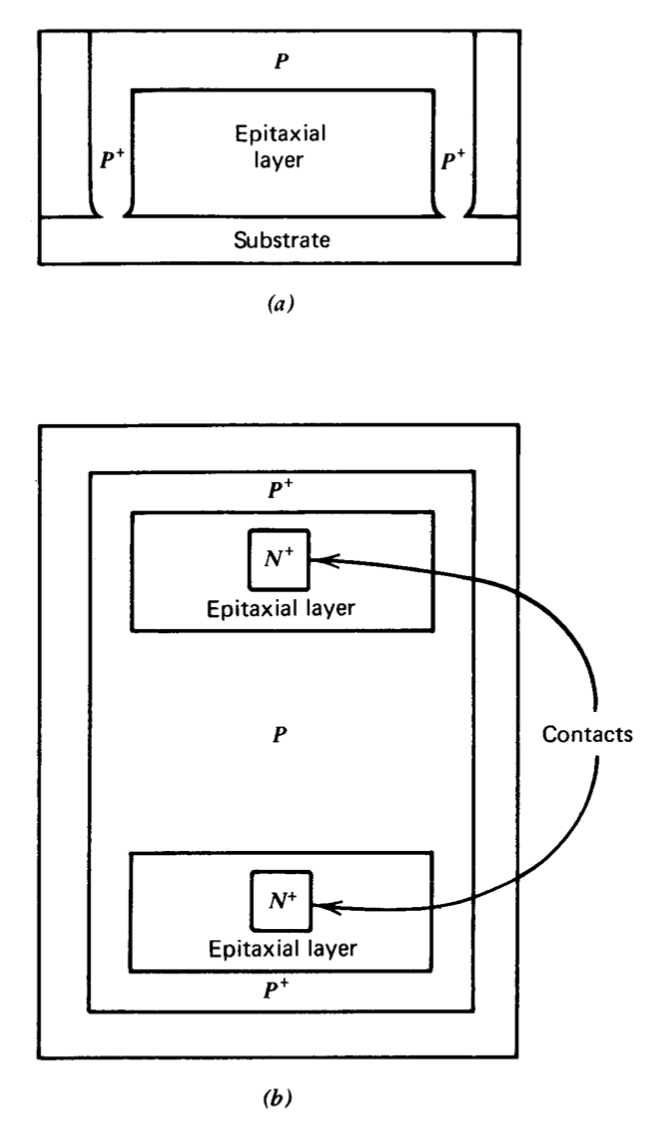
A second possible PNP structure is the vertical or substrate PNP illustrated in Figure 10.4. This type of transistor consists of an emitter formed by the NPN base diffusion and a base of NPN collector material, with the substrate forming the \(P\)-type collector. The base width is the difference between the depth of the \(P\)-type diffusion and the thickness of the epitaxial layer and can be controlled moderately well. Current gain can be reasonably high and bandwidth is considerably better than that of a lateral design. One un desirable consequence of the necessary compromises is that large-area tran sistors must be used to maintain gain at moderate current levels. Another more serious difficulty is that the collectors of all substrate PNP'S are com mon and are connected to the negative supply voltage. Thus substrate PNP'S can only be used as emitter followers.
Other Components
The \(P\)-type base material is normally used for resistors, and the resistivity of this material dictated by the base-region doping level is typically 100 to 200 ohms per square. Problems associated with achieving high length-to width ratios in a reasonable area and with tolerable distributed capacitance usually limit maximum resistance values to the order of 10 kilo-ohms. Similarly, other geometric considerations limit the lower value of resistors made using the base diffusion to the order of 25 ohms. Higher-value resistors (up to approximately 100 kilo-ohms) can be made using the higher-resistivity collector material, while lower-value resistors are formed from the heavily doped emitter material.
Practical considerations make control of absolute resistance values to better than 10 to 20% uneconomical, and the temperature coefficient of all integrated-circuit resistors is high by discrete-component standards. How ever, it is possible to match two resistors to 5 % or better, and all resistors made from one diffusion have identical temperature coefficients.
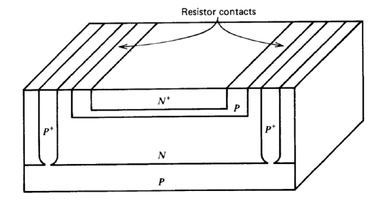
Figure 10.5 Pinched resistor.
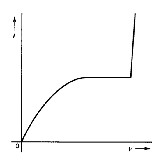
Figure 10.6 Pinched-resistor current-voltage characteristic.
It is possible to make large-value, small-geometry resistors by diffusing emitter material across a base-material resistor (see Figure 10.5). The cross-sectional area of the current path is decreased by this diffusion, and resistance values on the order of \(10 k\Omega\) per square are possible. The resultant device, called a pinched resistor, has the highly nonlinear characteristics illustrated in Figure 10.6. The lower-current portion of this curve results from field-effect transistor action, with the \(P\)-type resistor material forming a channel surrounded by an \(N\)-type gate. The potential of the gate region is maintained close to that of the most positive end of the channel by conduction through the \(P-N\) junction. Thus, if the positively biased end of the pinched resistor is considered the source of a \(P\)-channel FET, the characteristics of the resistor are the drain characteristics of a FET with approximately zero gate-to-source voltage. When the voltage applied across the structure exceeds the reverse breakdown voltage of the \(N^+\) and \(P\) junction, the heavily doped \(N^+\) region forms a low-resistance path across the resistor. The high-conductance region of the characteristics results from this effect.
In addition to the nonlinearity described above, the absolute value of a pinched resistor is considerably harder to control than that of a standard base-region resistor. In spite of these limitations, pinched resistors are used
in integrated circuits, often as shunt paths across base-to-emitter junctions of bipolar transistors. The absolute value of such a shunt path is relatively unimportant in many designs, and the voltage applied to the resistor is limited to a fraction of a volt by the transistor junction.
An alternative high-resistance structure that has been used as a bias current source in some integrated-circuit designs is the collector FET shown in Figure 10.7. This device, which acts as an \(N\)-channel FET with its gate biased at the negative supply voltage of circuit, does not have the breakdown-voltage problems associated with the pinched resistor.
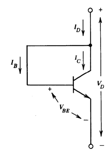
Integrated-circuit diodes are readily fabricated. The collector-to-base junction of NPN transistors can be used when moderately high reverse breakdown voltage is necessary. The diode-connected transistor (Figure 10.8) is used when diode characteristics matched to transistor characteristics are required. If it is assumed that the transistor terminal relationships are
\[I_C = I_S e^{qV_{BE}/kT} \nonumber \]
we can write for the diode-connected transistor
\[I_D = I_B + I_C = \left (1 + \dfrac{1}{\beta} \right ) I_C = \left (1 + \dfrac{1}{\beta} \right ) I_S e^{qV_D /kT} \simeq I_S e^{V_D /kT} \nonumber \]
The base-to-emitter junction is used as a Zener diode in some circuits. The reverse breakdown voltage of this junction is determined by transistor processing, with a typical value of six volts.
Reverse-biased diode junctions can be used as capacitors when the nonlinear characteristics of the space-charge-layer capacitance are acceptable. An alternative linear capacitor structure uses the oxide as a dielectric, with the aluminum metalization layer one plate and the semiconductor material the second plate. This type of metal-oxide-semiconductor capacitor has the further advantage of bipolar operation compared with a diode. The capacitance per unit area of either of these structures makes capacitors larger than \(100\ pF\) impractical.