
10.3: INTEGRATED-CIRCUIT DESIGN TECHNIQUES
- Page ID
- 58471

\( \newcommand{\vecs}[1]{\overset { \scriptstyle \rightharpoonup} {\mathbf{#1}} } \)
\( \newcommand{\vecd}[1]{\overset{-\!-\!\rightharpoonup}{\vphantom{a}\smash {#1}}} \)
\( \newcommand{\id}{\mathrm{id}}\) \( \newcommand{\Span}{\mathrm{span}}\)
( \newcommand{\kernel}{\mathrm{null}\,}\) \( \newcommand{\range}{\mathrm{range}\,}\)
\( \newcommand{\RealPart}{\mathrm{Re}}\) \( \newcommand{\ImaginaryPart}{\mathrm{Im}}\)
\( \newcommand{\Argument}{\mathrm{Arg}}\) \( \newcommand{\norm}[1]{\| #1 \|}\)
\( \newcommand{\inner}[2]{\langle #1, #2 \rangle}\)
\( \newcommand{\Span}{\mathrm{span}}\)
\( \newcommand{\id}{\mathrm{id}}\)
\( \newcommand{\Span}{\mathrm{span}}\)
\( \newcommand{\kernel}{\mathrm{null}\,}\)
\( \newcommand{\range}{\mathrm{range}\,}\)
\( \newcommand{\RealPart}{\mathrm{Re}}\)
\( \newcommand{\ImaginaryPart}{\mathrm{Im}}\)
\( \newcommand{\Argument}{\mathrm{Arg}}\)
\( \newcommand{\norm}[1]{\| #1 \|}\)
\( \newcommand{\inner}[2]{\langle #1, #2 \rangle}\)
\( \newcommand{\Span}{\mathrm{span}}\) \( \newcommand{\AA}{\unicode[.8,0]{x212B}}\)
\( \newcommand{\vectorA}[1]{\vec{#1}} % arrow\)
\( \newcommand{\vectorAt}[1]{\vec{\text{#1}}} % arrow\)
\( \newcommand{\vectorB}[1]{\overset { \scriptstyle \rightharpoonup} {\mathbf{#1}} } \)
\( \newcommand{\vectorC}[1]{\textbf{#1}} \)
\( \newcommand{\vectorD}[1]{\overrightarrow{#1}} \)
\( \newcommand{\vectorDt}[1]{\overrightarrow{\text{#1}}} \)
\( \newcommand{\vectE}[1]{\overset{-\!-\!\rightharpoonup}{\vphantom{a}\smash{\mathbf {#1}}}} \)
\( \newcommand{\vecs}[1]{\overset { \scriptstyle \rightharpoonup} {\mathbf{#1}} } \)
\( \newcommand{\vecd}[1]{\overset{-\!-\!\rightharpoonup}{\vphantom{a}\smash {#1}}} \)
\(\newcommand{\avec}{\mathbf a}\) \(\newcommand{\bvec}{\mathbf b}\) \(\newcommand{\cvec}{\mathbf c}\) \(\newcommand{\dvec}{\mathbf d}\) \(\newcommand{\dtil}{\widetilde{\mathbf d}}\) \(\newcommand{\evec}{\mathbf e}\) \(\newcommand{\fvec}{\mathbf f}\) \(\newcommand{\nvec}{\mathbf n}\) \(\newcommand{\pvec}{\mathbf p}\) \(\newcommand{\qvec}{\mathbf q}\) \(\newcommand{\svec}{\mathbf s}\) \(\newcommand{\tvec}{\mathbf t}\) \(\newcommand{\uvec}{\mathbf u}\) \(\newcommand{\vvec}{\mathbf v}\) \(\newcommand{\wvec}{\mathbf w}\) \(\newcommand{\xvec}{\mathbf x}\) \(\newcommand{\yvec}{\mathbf y}\) \(\newcommand{\zvec}{\mathbf z}\) \(\newcommand{\rvec}{\mathbf r}\) \(\newcommand{\mvec}{\mathbf m}\) \(\newcommand{\zerovec}{\mathbf 0}\) \(\newcommand{\onevec}{\mathbf 1}\) \(\newcommand{\real}{\mathbb R}\) \(\newcommand{\twovec}[2]{\left[\begin{array}{r}#1 \\ #2 \end{array}\right]}\) \(\newcommand{\ctwovec}[2]{\left[\begin{array}{c}#1 \\ #2 \end{array}\right]}\) \(\newcommand{\threevec}[3]{\left[\begin{array}{r}#1 \\ #2 \\ #3 \end{array}\right]}\) \(\newcommand{\cthreevec}[3]{\left[\begin{array}{c}#1 \\ #2 \\ #3 \end{array}\right]}\) \(\newcommand{\fourvec}[4]{\left[\begin{array}{r}#1 \\ #2 \\ #3 \\ #4 \end{array}\right]}\) \(\newcommand{\cfourvec}[4]{\left[\begin{array}{c}#1 \\ #2 \\ #3 \\ #4 \end{array}\right]}\) \(\newcommand{\fivevec}[5]{\left[\begin{array}{r}#1 \\ #2 \\ #3 \\ #4 \\ #5 \\ \end{array}\right]}\) \(\newcommand{\cfivevec}[5]{\left[\begin{array}{c}#1 \\ #2 \\ #3 \\ #4 \\ #5 \\ \end{array}\right]}\) \(\newcommand{\mattwo}[4]{\left[\begin{array}{rr}#1 \amp #2 \\ #3 \amp #4 \\ \end{array}\right]}\) \(\newcommand{\laspan}[1]{\text{Span}\{#1\}}\) \(\newcommand{\bcal}{\cal B}\) \(\newcommand{\ccal}{\cal C}\) \(\newcommand{\scal}{\cal S}\) \(\newcommand{\wcal}{\cal W}\) \(\newcommand{\ecal}{\cal E}\) \(\newcommand{\coords}[2]{\left\{#1\right\}_{#2}}\) \(\newcommand{\gray}[1]{\color{gray}{#1}}\) \(\newcommand{\lgray}[1]{\color{lightgray}{#1}}\) \(\newcommand{\rank}{\operatorname{rank}}\) \(\newcommand{\row}{\text{Row}}\) \(\newcommand{\col}{\text{Col}}\) \(\renewcommand{\row}{\text{Row}}\) \(\newcommand{\nul}{\text{Nul}}\) \(\newcommand{\var}{\text{Var}}\) \(\newcommand{\corr}{\text{corr}}\) \(\newcommand{\len}[1]{\left|#1\right|}\) \(\newcommand{\bbar}{\overline{\bvec}}\) \(\newcommand{\bhat}{\widehat{\bvec}}\) \(\newcommand{\bperp}{\bvec^\perp}\) \(\newcommand{\xhat}{\widehat{\xvec}}\) \(\newcommand{\vhat}{\widehat{\vvec}}\) \(\newcommand{\uhat}{\widehat{\uvec}}\) \(\newcommand{\what}{\widehat{\wvec}}\) \(\newcommand{\Sighat}{\widehat{\Sigma}}\) \(\newcommand{\lt}{<}\) \(\newcommand{\gt}{>}\) \(\newcommand{\amp}{&}\) \(\definecolor{fillinmathshade}{gray}{0.9}\)Most high-volume manufacturers of integrated circuits have chosen to live with the limitations of the six-mask process in order to enjoy the associated economy. This process dictates circuit considerations beyond those implied by the limited spectrum of component types. For example, large-value base-material resistors or capacitors require a disproportionate share of the total chip area of a circuit. Since defects occur with a per-unit-area probability, the use of larger areas that decrease the yield of the process and thus increase production cost are to be avoided.
The designers of integrated operational amplifiers try to make maximum use of the advantages of integrated processing such as the large number of transistors that can be economically included in each circuit and the excellent match and thermal equality that can be achieved among various components in order to circumvent its limitations. The remarkable performance of presently available designs is a tribute to their success in achieving this objective. This section describes some of the circuit configurations that have evolved from this type of design effort.
Current Repeaters
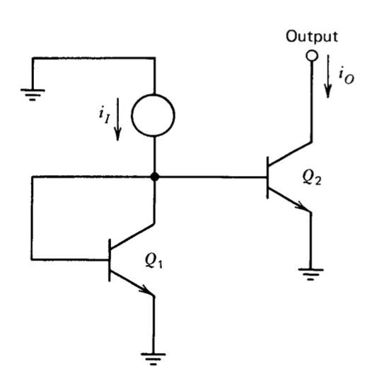
Many linear integrated circuits use a connection similar to that shown in Figure 10.9, either for biasing or as a controlled current source. Assume that both transistors have identical values for saturation current \(I_S\) and that \(\beta\) is high so that base currents of both transistors can be neglected. In this case, the collector current of \(Q_1\) is equal to \(i_I\). Since the base-to-emitter voltages of \(Q_1\) and \(Q_2\) are identical, currents \(i_I\) and \(i_O\) must be equal.(In the discussion of this and other current-repeater connections it is assumed that the output terminal voltage is such that the output transistor is in its forward operating region. Note that it is not necessary to have the driving current \(i_I\) supplied from a current source. In many actual designs, this current is supplied from a voltage source via a resistor or from another active device.) An alternative is to change the relative areas of \(Q_1\) and \(Q_2\). This geometric change results in a directly proportional change in saturation currents, so that currents \(i_I\) and \(i_O\) become a controlled multiple of each other. If \(i_I\) is made constant, transistor \(Q_2\) functions as a current source for voltages to within approximately \(100\ mV\) of ground. This performance permits the dynamic voltage range of many designs to be nearly equal to the supply voltage.
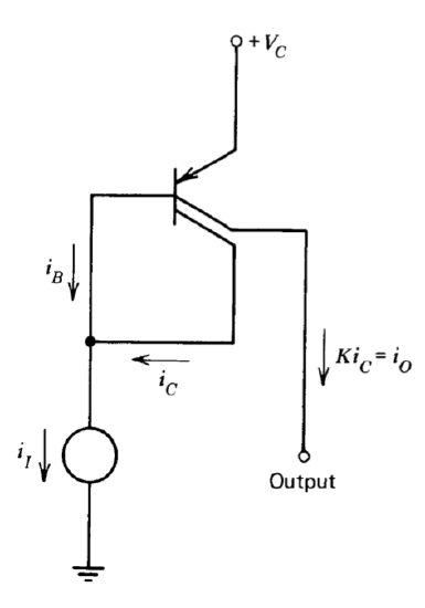
The split-collector lateral PNP transistor described earlier functions as a current repeater when connected as shown in Figure 10.10. The constant \(K\) that relates the two collector currents in this connection depends on the relative sizes of the collector segments. Since the base current for the lateral PNP is equal to the sum of the two collector currents divided by its current gain \(\beta_P\), we can write
\[i_I = i_B + i_C = i_C \dfrac{(1 + K)}{\beta_P} + i_C\label{eq10.3.1} \]
and
\[i_O = Ki_C\label{eq10.3.2} \]
Combining Equations \(\ref{eq10.3.1}\) and \(\ref{eq10.3.2}\) shows that the current gain for this connection is
\[\dfrac{i_O}{i_I} = \dfrac{K}{1+[(1+K)/\beta_P]} \nonumber \]
If values are selected so that \(1 + K \ll \beta_P\), the feedback inherent to this connection makes its input-output transfer ratio relatively insensitive to changes in \(\beta_P\). This desensitivity is advantageous since the quantity \(K\), determined by mask geometry, is significantly better controlled than is \(\beta_P\). The feedback also increases the current-gain half-power frequency of the controlled-gain PNP above the \(\beta\) cutoff frequency of the lateral-PNP transis tor itself.
The simple current repeater shown in Figure 10.9 is frequently augmented to make its current transfer ratio less sensitive to changes in transistor parameters. Equal-value emitter resistors can be included to stabilize the transfer ratio of the connection for changes in the base-to-emitter voltages of the two transistors. While this technique is sometimes used for discrete-component current repeaters, it is of questionable value in many integrated designs because matched resistors are as difficult to fabricate as matched transistors.
Other modifications are intended to reduce the dependency of the current transfer ratio on the transistor current gain. It is easily shown that the current transfer ratio for Figure 10.9, assuming perfectly matched transistors, is
\[\dfrac{i_O}{i_I} = \dfrac{1}{1 + 2/beta} \nonumber \]
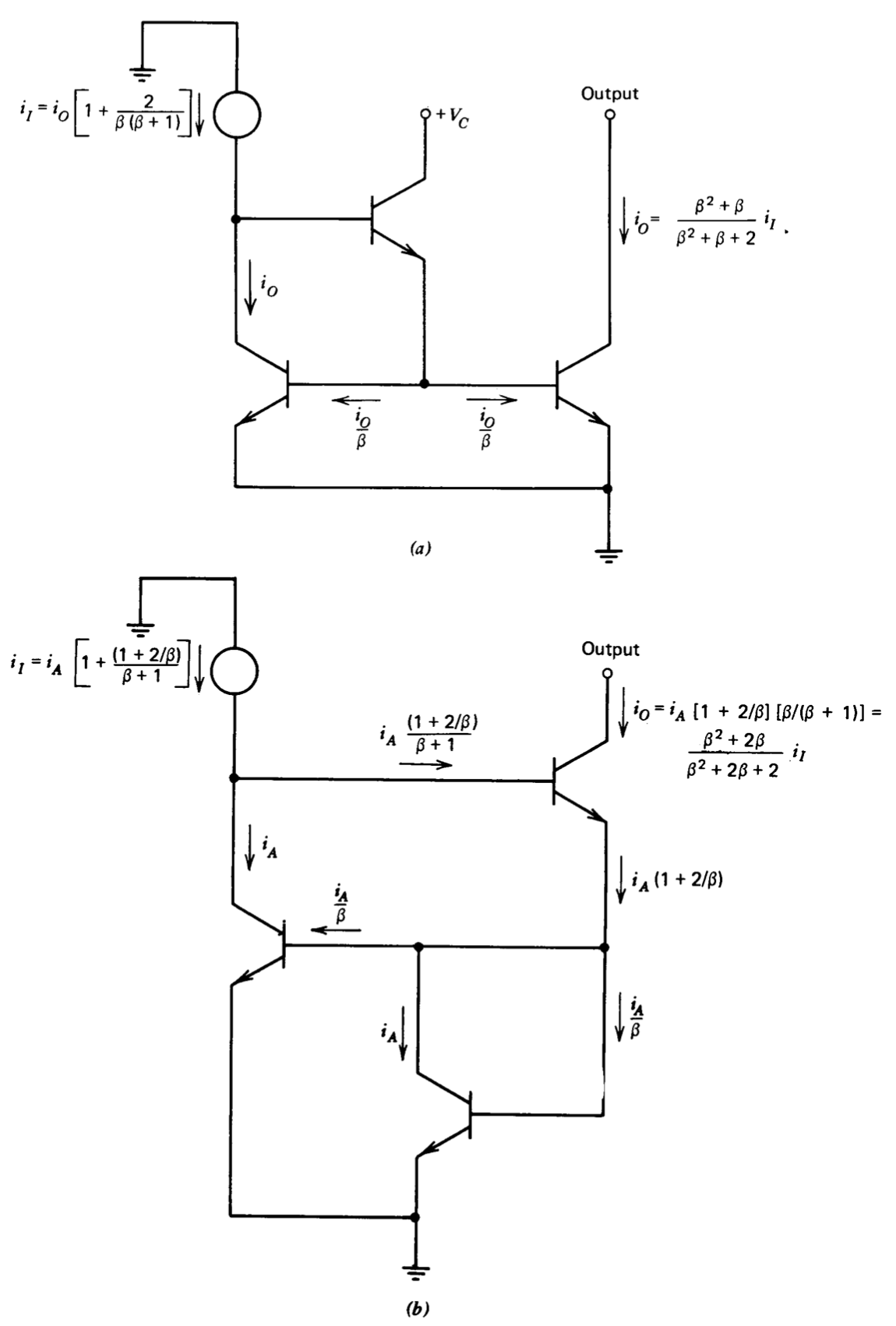
Figure 10.11 shows two somewhat more complex current-repeater connections assumed constructed with perfectly matched transistors. Intermediate currents that facilitate calculation of current transfer ratios are included in these diagrams. The circuit of Figure 10.11\(a\) uses an emitter follower to buffer the base currents of a conventional current repeater. The resultant current transfer ratio is
\[\dfrac{i_O}{i_I} = \dfrac{1}{1 + 2/[\beta (\beta + 1)]} = \dfrac{\beta^2 + \beta}{\beta^2 + \beta + 2} \nonumber \]
The connection of Figure 10.11\(b\) uses an interesting current cancellation technique to obtain a transfer ratio
\[\dfrac{i_O}{i_I} = \dfrac{[1 + 2/\beta][\beta /(\beta + 1)]}{1 + (1 + 2/\beta )/(\beta + 1)} = \dfrac{\beta^2 + 2\beta}{\beta^2 + 2\beta + 2} \nonumber \]
Either of these currents repeaters has a transfer ratio that differs from unity by a factor of approximately \((1 + 2 /\beta^2)\) compared with a factor of \((1 + 2/\beta )\) for the circuit of Figure 10.9, and are thus considerably less sensitive to variations in \(\beta\). It can also be shown (see Problem P10.5) that the output resistance of the circuit illustrated in Figure 10.11\(b\) is the order of \(r_{\mu}\) while that of either of the other circuits is the order of \(r_o\). This difference is significant in some high-gain connections.
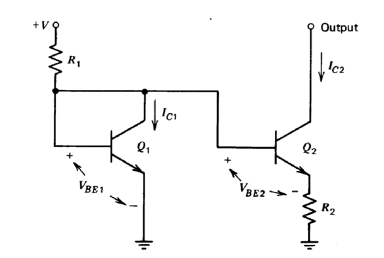
A clever modification of the current repeater, first used in the 709 design, yields a low-value constant-current source using only moderate-value resistors. Assuming high \(\beta\) and a large value of \(V\) relative to \(V_{BE1}\) in Figure 10.12,
\[I_{C1} \simeq \dfrac{V}{R_1} \nonumber \]
so that
\[V_{BE1} \simeq \dfrac{kT}{q} \ln \dfrac{V}{R_1 I_{S1}}\label{eq10.3.8} \]
However,
\[I_{C2} R_2 + \dfrac{kT}{q} \ln \dfrac{I_{C2}}{I_{S_2}} = V_{BE1}\label{eq10.3.9} \]
If it is assumed that saturation currents are equal, combining Equations \(\ref{eq10.3.8}\) and \(\ref{eq10.3.9}\) yields
\[I_{C2} R_2 = \dfrac{kT}{q} \ln \dfrac{V}{R_1I_{C2}}\label{eq10.3.10} \]
The resultant transcendental equation can be solved for any particular choice of constants. For example, if Equation \(\ref{eq10.3.10}\) is evaluated at room temperature \((kT/q \simeq 26mV)\) for \(V/R_1 =1\ mA\) and \(R_2 = 12k\Omega\), \(I_{C2} \simeq 10 \mu A\).
Other Connections
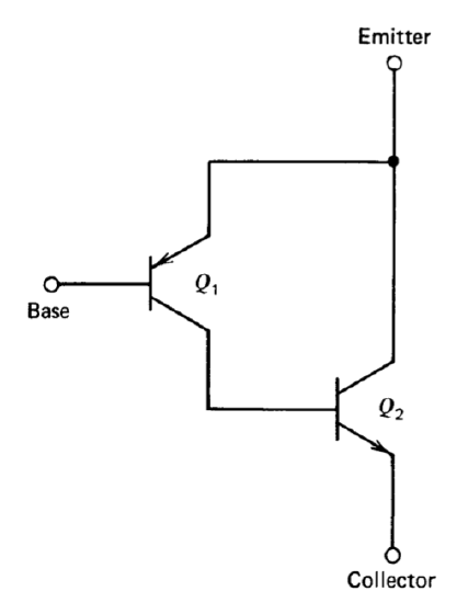
Most operational-amplifier designs require both NPN and PNP transistors in order to provide voltage level shifting. Several connections effectively augment the low gain of many lateral PNP designs by combining the PNP transistor with an NPN transistor as shown in Figure 10.13. (This connection is also used in discrete-component circuits and is called the complementary Darlington connection.) At low frequencies this combination appears as a single PNP transistor with the base, emitter, and collector terminals as indicated. The current gain of this compound transistor is approximately equal to the product of the gains of the two individual devices, while trans-conductance is related to collector current of the combination as in a conventional transistor.
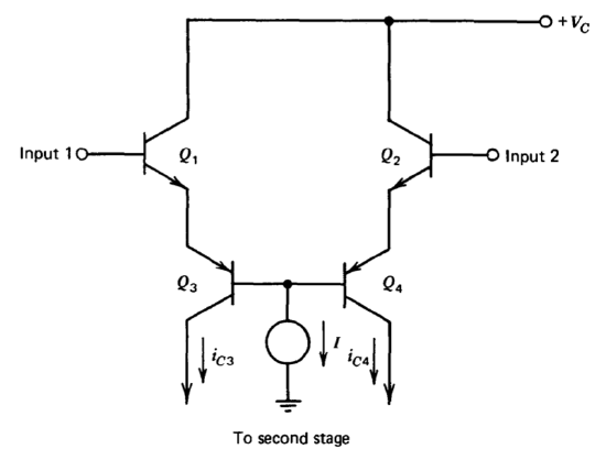
An ingenious connection using lateral PNP transistors, shown in Figure 10.14, was introduced in the LM101 amplifier design. Assume that the two NPN transistors have identical saturation currents, as do the PNP's. Further
assume that the current gains of both PNP transistors are \(\beta_P\). The total output collector current, \(i_{C3} + i_{C4}\), must be equal to \(\beta_P I\). If the input voltages are equal, \(i_{C3}\) and \(i_{C4}\) must be equal because of the matched saturation currents. As a differential input signal is applied, the relative collector currents change differentially; therefore this stage can be used to perform the circuit function of a differential pair of PNP transistors. However, the ratio of input current to collector current depends on the current gain of the high-gain NPN's. Another advantage is that the input capacitance is low since the input transistors are operating as emitter followers. Furthermore, the low-bandwidth PNP devices are operating in an incrementally grounded-base connection for differential input signals, and this connection maximizes their bandwidth in the circuit. One disadvantage is that the series connection of four base-to-emitter junctions lowers transconductance by a factor of two compared to a standard differential amplifier operating at the same quiescent current level.
It is interesting to note that the successful operation of this circuit is actually dependent on the low gain characteristic of the lateral-PNP transistors used. If high-gain transistors were used, capacitive loading at the bases of the two PNP transistors would cause large collector currents as a function of the time rate of change of common-mode level. The controlled gain PNP shown in Figure 10.10 is used in this connection in some modern amplifier designs.
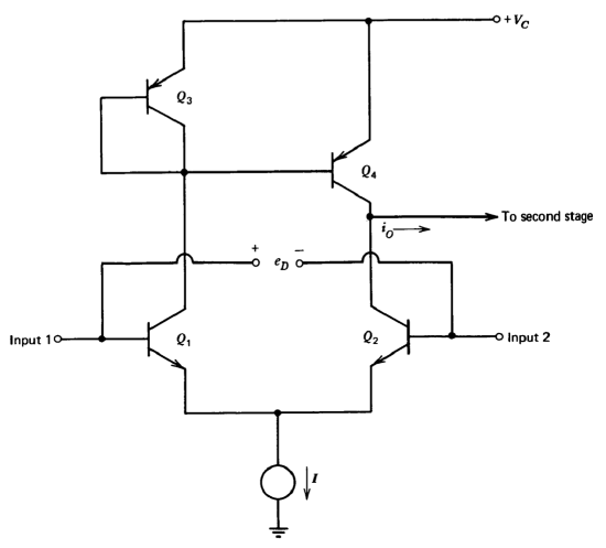
Several connections are used to double the effective transconductance of an input differential pair and thus increase the gain provided by this portion of an operational amplifier. One such circuit is shown in Figure 10.15. Assume equal operating currents for \(Q_1\) and \(Q_2\). If \(Q_4\) were a constant current source, the incremental output current would be related to a differential input voltage ed as \(i_o/e_d = g_m/2\). The differential connection of \(Q_1\) and \(Q_2\) insures that incremental changes in collector currents of these devices are equal in magnitude but opposite in polarity, and the current repeater connection of \(Q_3\) and \(Q_4\) effectively subtracts the change in collector current of \(Q_1\) from that of \(Q_2\). (The more sophisticated current repeaters described in the last section are often substituted.) The gain is increased by a factor of two so that \(i_o/e_d = g_m\). Another advantage is that the impedance level at the circuit output is high so that this stage can provide high voltage gain if required. We will see that some integrated-circuit operational amplifiers exploit this possibility to distribute the total gain more equally between the two stages than was done with the discrete-component design discussed in the last chapter.
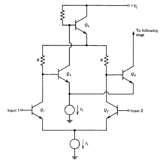
Another approach is illustrated in Figure 10.16. A differential input causes equal-magnitude changes in the collector currents of \(Q_1\) and \(Q_2\). However, the high gain of the \(Q_3-Q_5\) loop changes the voltage at the emitter of \(Q_5\) in such a way as to minimize current changes at the base of \(Q_3\). Thus the current through the load resistor for \(Q_1\) is changed by an amount approximately equal to the change in \(i_{C1}\). A corresponding change occurs in the current through the load resistor for \(Q_2\), doubling the current into the base of \(Q_4\).