
12.2: NONLINEAR OSCILLATORS
- Page ID
- 58478
\( \newcommand{\vecs}[1]{\overset { \scriptstyle \rightharpoonup} {\mathbf{#1}} } \)
\( \newcommand{\vecd}[1]{\overset{-\!-\!\rightharpoonup}{\vphantom{a}\smash {#1}}} \)
\( \newcommand{\dsum}{\displaystyle\sum\limits} \)
\( \newcommand{\dint}{\displaystyle\int\limits} \)
\( \newcommand{\dlim}{\displaystyle\lim\limits} \)
\( \newcommand{\id}{\mathrm{id}}\) \( \newcommand{\Span}{\mathrm{span}}\)
( \newcommand{\kernel}{\mathrm{null}\,}\) \( \newcommand{\range}{\mathrm{range}\,}\)
\( \newcommand{\RealPart}{\mathrm{Re}}\) \( \newcommand{\ImaginaryPart}{\mathrm{Im}}\)
\( \newcommand{\Argument}{\mathrm{Arg}}\) \( \newcommand{\norm}[1]{\| #1 \|}\)
\( \newcommand{\inner}[2]{\langle #1, #2 \rangle}\)
\( \newcommand{\Span}{\mathrm{span}}\)
\( \newcommand{\id}{\mathrm{id}}\)
\( \newcommand{\Span}{\mathrm{span}}\)
\( \newcommand{\kernel}{\mathrm{null}\,}\)
\( \newcommand{\range}{\mathrm{range}\,}\)
\( \newcommand{\RealPart}{\mathrm{Re}}\)
\( \newcommand{\ImaginaryPart}{\mathrm{Im}}\)
\( \newcommand{\Argument}{\mathrm{Arg}}\)
\( \newcommand{\norm}[1]{\| #1 \|}\)
\( \newcommand{\inner}[2]{\langle #1, #2 \rangle}\)
\( \newcommand{\Span}{\mathrm{span}}\) \( \newcommand{\AA}{\unicode[.8,0]{x212B}}\)
\( \newcommand{\vectorA}[1]{\vec{#1}} % arrow\)
\( \newcommand{\vectorAt}[1]{\vec{\text{#1}}} % arrow\)
\( \newcommand{\vectorB}[1]{\overset { \scriptstyle \rightharpoonup} {\mathbf{#1}} } \)
\( \newcommand{\vectorC}[1]{\textbf{#1}} \)
\( \newcommand{\vectorD}[1]{\overrightarrow{#1}} \)
\( \newcommand{\vectorDt}[1]{\overrightarrow{\text{#1}}} \)
\( \newcommand{\vectE}[1]{\overset{-\!-\!\rightharpoonup}{\vphantom{a}\smash{\mathbf {#1}}}} \)
\( \newcommand{\vecs}[1]{\overset { \scriptstyle \rightharpoonup} {\mathbf{#1}} } \)
\(\newcommand{\longvect}{\overrightarrow}\)
\( \newcommand{\vecd}[1]{\overset{-\!-\!\rightharpoonup}{\vphantom{a}\smash {#1}}} \)
\(\newcommand{\avec}{\mathbf a}\) \(\newcommand{\bvec}{\mathbf b}\) \(\newcommand{\cvec}{\mathbf c}\) \(\newcommand{\dvec}{\mathbf d}\) \(\newcommand{\dtil}{\widetilde{\mathbf d}}\) \(\newcommand{\evec}{\mathbf e}\) \(\newcommand{\fvec}{\mathbf f}\) \(\newcommand{\nvec}{\mathbf n}\) \(\newcommand{\pvec}{\mathbf p}\) \(\newcommand{\qvec}{\mathbf q}\) \(\newcommand{\svec}{\mathbf s}\) \(\newcommand{\tvec}{\mathbf t}\) \(\newcommand{\uvec}{\mathbf u}\) \(\newcommand{\vvec}{\mathbf v}\) \(\newcommand{\wvec}{\mathbf w}\) \(\newcommand{\xvec}{\mathbf x}\) \(\newcommand{\yvec}{\mathbf y}\) \(\newcommand{\zvec}{\mathbf z}\) \(\newcommand{\rvec}{\mathbf r}\) \(\newcommand{\mvec}{\mathbf m}\) \(\newcommand{\zerovec}{\mathbf 0}\) \(\newcommand{\onevec}{\mathbf 1}\) \(\newcommand{\real}{\mathbb R}\) \(\newcommand{\twovec}[2]{\left[\begin{array}{r}#1 \\ #2 \end{array}\right]}\) \(\newcommand{\ctwovec}[2]{\left[\begin{array}{c}#1 \\ #2 \end{array}\right]}\) \(\newcommand{\threevec}[3]{\left[\begin{array}{r}#1 \\ #2 \\ #3 \end{array}\right]}\) \(\newcommand{\cthreevec}[3]{\left[\begin{array}{c}#1 \\ #2 \\ #3 \end{array}\right]}\) \(\newcommand{\fourvec}[4]{\left[\begin{array}{r}#1 \\ #2 \\ #3 \\ #4 \end{array}\right]}\) \(\newcommand{\cfourvec}[4]{\left[\begin{array}{c}#1 \\ #2 \\ #3 \\ #4 \end{array}\right]}\) \(\newcommand{\fivevec}[5]{\left[\begin{array}{r}#1 \\ #2 \\ #3 \\ #4 \\ #5 \\ \end{array}\right]}\) \(\newcommand{\cfivevec}[5]{\left[\begin{array}{c}#1 \\ #2 \\ #3 \\ #4 \\ #5 \\ \end{array}\right]}\) \(\newcommand{\mattwo}[4]{\left[\begin{array}{rr}#1 \amp #2 \\ #3 \amp #4 \\ \end{array}\right]}\) \(\newcommand{\laspan}[1]{\text{Span}\{#1\}}\) \(\newcommand{\bcal}{\cal B}\) \(\newcommand{\ccal}{\cal C}\) \(\newcommand{\scal}{\cal S}\) \(\newcommand{\wcal}{\cal W}\) \(\newcommand{\ecal}{\cal E}\) \(\newcommand{\coords}[2]{\left\{#1\right\}_{#2}}\) \(\newcommand{\gray}[1]{\color{gray}{#1}}\) \(\newcommand{\lgray}[1]{\color{lightgray}{#1}}\) \(\newcommand{\rank}{\operatorname{rank}}\) \(\newcommand{\row}{\text{Row}}\) \(\newcommand{\col}{\text{Col}}\) \(\renewcommand{\row}{\text{Row}}\) \(\newcommand{\nul}{\text{Nul}}\) \(\newcommand{\var}{\text{Var}}\) \(\newcommand{\corr}{\text{corr}}\) \(\newcommand{\len}[1]{\left|#1\right|}\) \(\newcommand{\bbar}{\overline{\bvec}}\) \(\newcommand{\bhat}{\widehat{\bvec}}\) \(\newcommand{\bperp}{\bvec^\perp}\) \(\newcommand{\xhat}{\widehat{\xvec}}\) \(\newcommand{\vhat}{\widehat{\vvec}}\) \(\newcommand{\uhat}{\widehat{\uvec}}\) \(\newcommand{\what}{\widehat{\wvec}}\) \(\newcommand{\Sighat}{\widehat{\Sigma}}\) \(\newcommand{\lt}{<}\) \(\newcommand{\gt}{>}\) \(\newcommand{\amp}{&}\) \(\definecolor{fillinmathshade}{gray}{0.9}\)The discussion of oscillators up to this point has focused on the design of circuits that provide sinusoidal output signals. The basic approach is to use a linear, second-order feedback loop to generate the sinusoid, and then incorporate some mechanism to control amplitude.
Operational amplifiers are also frequently used in nonlinear oscillator circuits that intentionally produce nonsinusoidal output signals. The analy sis of these types of oscillators is complicated by the fact that transform methods normally cannot be used. One frequently used technique for evaluating the performance of these types of oscillators is to determine the output and internal signals directly via time-domain calculations.
Square- and Triangle-Wave Generator
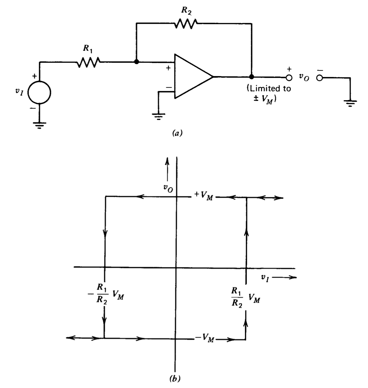
A function generator that produces square and triangle waves as its outputs was used as an example of describing-function analysis in Section 6.3.3. This topology combines an integrator with a Schmitt-trigger circuit. The Schmitt trigger can be realized by applying positive feedback around an operational amplifier, as shown in Figure 12.7.(In many practical circuits, a comparator rather than an operational amplifier is used to implement a Schmitt trigger. A comparator, like an operational amplifier, is a high-gain, direct-coupled amplifier. However, since it is riot intended for use in negative-feedback connections, the frequency-response compromises that must be made to insure the stability of an operational amplifier need not be included in the comparator design. Consequently, the response time of a Schmitt trigger realized via a comparator can be significantly faster than that obtained using an operational amplifier.) Consider operation with \(v_I\) a large positive voltage. In this case the amplifier will be saturated with a positive output voltage.
It is assumed that the output-voltage magnitude is limited to a maximum value of \(V_M\). This limiting can be accomplished in several ways. If relatively crude level control is sufficient, the saturation levels may be determined simply by power-supply voltages and internal amplifier voltage drops. Somewhat better control is possible if an amplifier such as the LM101A (see Section 10.4.1) is used. The output level of this circuit can be limited by connecting diode clamps to a compensation terminal. A third possibility is to follow the operational amplifier shown with a precision limiter similar to those described in Section 11.5.3, and to apply positive feedback around the entire connection. This approach has the further advantage that the output element is operating with local negative feedback and thus has very low output resistance.
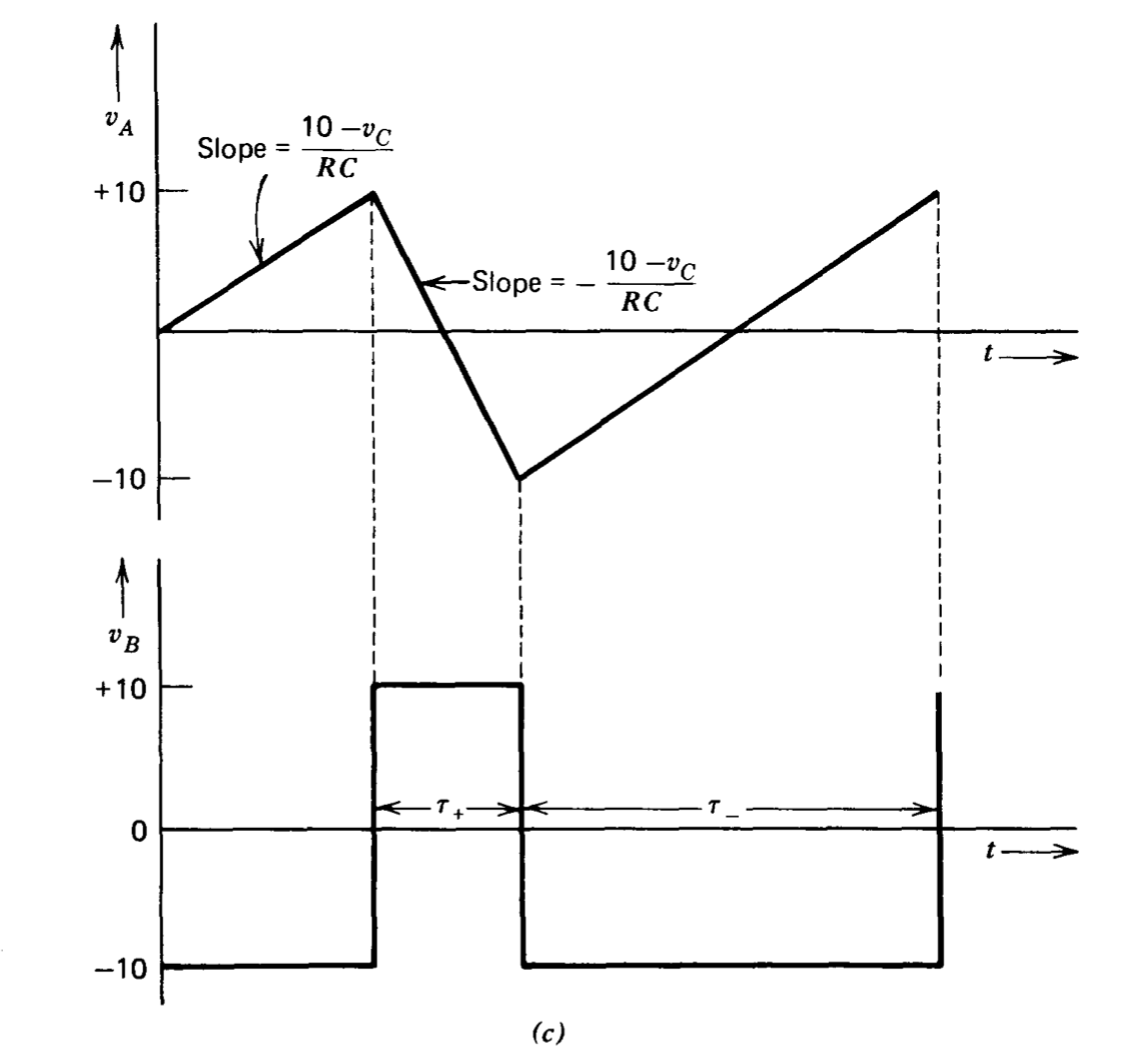
In order to force the circuit to change state, the input voltage is lowered. When the input level reaches approximately \(- (R_1/R_2) V_M\), the noninverting input of the amplifier is close to ground potential and the device enters its linear operating region. The massive positive feedback that results with the amplifier active sweeps its output negative until a level of \(-V_M\) is reached. Further negative changes in input voltage do not affect the output. If the input voltage is raised, the amplifier enters its active region at an input level of \(+(R_1/R_2)V_M\), and is then driven to positive saturation. These transition points combine to give the characteristics shown in Figure 12.7\(b\). A possible oscillator connection using this type of Schmitt trigger is shown in Figure 12.8. With the modulating voltage \(v_C = 0\), signal waveforms are as shown in part \(b\) of this figure. The period of oscillation is determined by noting that the magnitude of the slope of the triangle wave is always \(10/RC\), and that the total change in the voltate level of \(v_A\) is 40 volts for one complete cycle. Therefore
\[\tau = \dfrac{40}{10/RC} = 4RC \nonumber \]
The corresponding frequency of oscillation is
\[f = \dfrac{1}{\tau} = \dfrac{1}{4RC} \nonumber \]
In commercial versions of this circuit, decade frequency switching is frequently accomplished by changing capacitors, while variation of the value of resistor \(R\) provides vernier control in any one decade.
Duty-Cycle Modulation
The current that charges the capacitor can be modulated by means of an applied voltage \(v_C\), with this current given by
\[i_A = \dfrac{v_C + v_B}{R} \nonumber \]
A positive value for \(v_C\) increases capacitor charging current when \(v_B\) is positive and decreases this current when \(v_B\) is negative. The net result is to duty-cycle modulate the signal \(v_B\) as shown in Figure 12.8\(c\). The fraction of the time this signal stays positive is
\[\dfrac{r_+}{r_+ + r_-} = \dfrac{20RC/(10 + v_C)}{20RC/(10 + v_C) + 20RC/(10 - v_C)} = \dfrac{1}{2} \left (1 - \dfrac{v_C}{10} \right ) \label{eq12.2.4} \]
This duty-cycle modulator has a number of interesting features that make it useful in a variety of applications. Equation \(\ref{eq12.2.4}\) shows that the duty cycle is linearly proportional to vc and changes from one to zero as \(v_C\) changes from - 10 volts to +10 volts. However, maximum capacitor charging current is limited to twice its value with zero \(v_C\), so that the time spent in the shorter of the two periods is never less than half its quiescent value. The frequency of operation is a nonlinear function of \(v_C\) and is given by
\[f = \dfrac{1}{r_+ + r_-} = \dfrac{1}{20RC/(10 + v_C) + 20RC/(10 - v_C)} = \dfrac{100 - v_C^2}{400RC} \nonumber \]
This equation shows that the frequency is lowered by any nonzero value of \(v_C\).
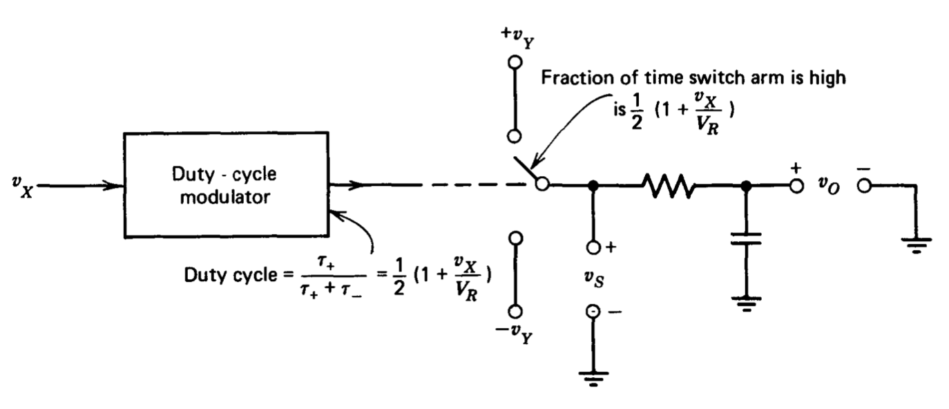
Applications include the control of switching power amplifiers and the realization of the type of analog multiplier shown in Figure 12.9. In this circuit, the duty-cycle modulator controls the state of a switch that is frequently realized with field-effect transistors. The circuit is arranged so that the switch arm is connected to a voltage \(+v_Y\) for a fraction of the time \(\tfrac{1}{2} [1 + (v_X/V_R)]\), and to a voltage \(-v_Y\) for the remainder of the time, a fraction equal to \(\tfrac{1}{2} [1 - (v_X/V_R)]\). (Alternative implementations use current rather than voltage switching to increase switching speed.) The output filter (usually a multiple-order active filter rather than the simple network shown) averages the switch voltage \(v_S\), so that
\[v_O = \overline{v_S} = + v_Y \left [ \dfrac{1}{2} \left ( 1 + \dfrac{v_X}{V_R} \right ) \right ] - v_Y \left [ \dfrac{1}{2} \left ( 1 - \dfrac{v_X}{V_R} \right ) \right ] = \dfrac{v_X v_Y}{V_R} \nonumber \]
where the over bar indicates time averaging. Note that the voltage \(V_R\) (which is equal to the maximum magnitude of the signal out of the Schmitt trigger) can be varied to mechanize division. A technique for varying the signal from the Schmitt trigger is described below.
Versions of this type of multiplier that limit errors to 0.05 % of maximum output have been designed.
Frequency Modulation
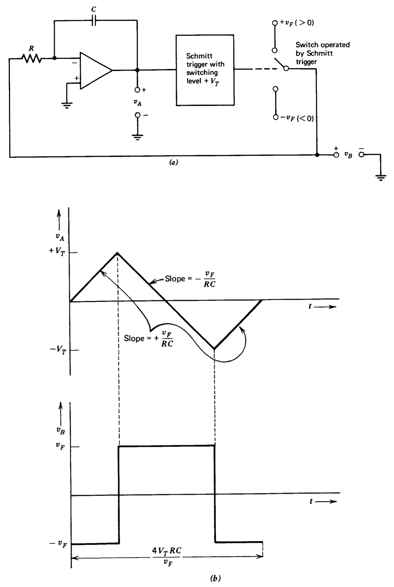
Another variation of the basic nonlinear oscillator shown in Figure 12.10 results in an oscillator with a voltage-controlled operating frequency. Here the Schmitt trigger determines the state of a switch that allows a variable-level voltage to be applied to the integrator. If the Schmitt trigger switches at input-signal levels of \(\pm V_T\) the total excursion of the signal \(v_A\) will be \(4\ V_T\) volts per cycle. The slope of signal \(v_A\) has a magnitude of \(v_F/RC\) volts per second, and thus the frequency of oscillation is
\[f = \dfrac{v_F/RC}{4V_T} = \dfrac{v_F}{4V_T RC} \nonumber \]
Single-Amplifier Nonlinear Oscillator
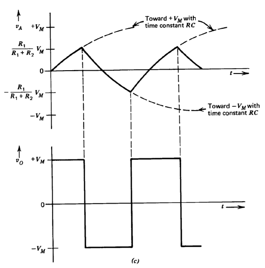
The operational amplifier used as an integrator in the nonlinear oscillator described above can be replaced with a passive resistor-capacitor network a shown in Figure 12.11, resulting in a configuration first reported by Bose.(A. G. Bose, "ATwo-State Modulation System," 1963 Wescon Convention Record, Part 6, Paper 7.1. ) The Schmitt trigger functions in an inverting mode in this connection so that a sufficiently positive level for \(v_A\) saturates the amplifier output at \(-V_M\). Switching points occur at \(VA = \pm V_M R_1/(R_1 + R_2)\). If the dotted modulating resistor is omitted, the waveforms are as shown in Figure 12.11\(c\). The capacitor voltage is a sequence of exponential segments rather than a true triangular wave. The duty cycle of the signal can be modulated by including the dotted resistor shown in Figure 12.11\(a\). If the width of the hysterisis region is made very small by choosing \(R_1 \ll R_2\), the current into the capacitor becomes nearly constant in each state, since the circuit keeps the capacitor voltage close to zero. In this case, the duty cycle of the voltage \(v_O\) is linearly related to control voltage \(v_C\).