
12.3: ANALOG COMPUTATION
- Page ID
- 58479
\( \newcommand{\vecs}[1]{\overset { \scriptstyle \rightharpoonup} {\mathbf{#1}} } \)
\( \newcommand{\vecd}[1]{\overset{-\!-\!\rightharpoonup}{\vphantom{a}\smash {#1}}} \)
\( \newcommand{\dsum}{\displaystyle\sum\limits} \)
\( \newcommand{\dint}{\displaystyle\int\limits} \)
\( \newcommand{\dlim}{\displaystyle\lim\limits} \)
\( \newcommand{\id}{\mathrm{id}}\) \( \newcommand{\Span}{\mathrm{span}}\)
( \newcommand{\kernel}{\mathrm{null}\,}\) \( \newcommand{\range}{\mathrm{range}\,}\)
\( \newcommand{\RealPart}{\mathrm{Re}}\) \( \newcommand{\ImaginaryPart}{\mathrm{Im}}\)
\( \newcommand{\Argument}{\mathrm{Arg}}\) \( \newcommand{\norm}[1]{\| #1 \|}\)
\( \newcommand{\inner}[2]{\langle #1, #2 \rangle}\)
\( \newcommand{\Span}{\mathrm{span}}\)
\( \newcommand{\id}{\mathrm{id}}\)
\( \newcommand{\Span}{\mathrm{span}}\)
\( \newcommand{\kernel}{\mathrm{null}\,}\)
\( \newcommand{\range}{\mathrm{range}\,}\)
\( \newcommand{\RealPart}{\mathrm{Re}}\)
\( \newcommand{\ImaginaryPart}{\mathrm{Im}}\)
\( \newcommand{\Argument}{\mathrm{Arg}}\)
\( \newcommand{\norm}[1]{\| #1 \|}\)
\( \newcommand{\inner}[2]{\langle #1, #2 \rangle}\)
\( \newcommand{\Span}{\mathrm{span}}\) \( \newcommand{\AA}{\unicode[.8,0]{x212B}}\)
\( \newcommand{\vectorA}[1]{\vec{#1}} % arrow\)
\( \newcommand{\vectorAt}[1]{\vec{\text{#1}}} % arrow\)
\( \newcommand{\vectorB}[1]{\overset { \scriptstyle \rightharpoonup} {\mathbf{#1}} } \)
\( \newcommand{\vectorC}[1]{\textbf{#1}} \)
\( \newcommand{\vectorD}[1]{\overrightarrow{#1}} \)
\( \newcommand{\vectorDt}[1]{\overrightarrow{\text{#1}}} \)
\( \newcommand{\vectE}[1]{\overset{-\!-\!\rightharpoonup}{\vphantom{a}\smash{\mathbf {#1}}}} \)
\( \newcommand{\vecs}[1]{\overset { \scriptstyle \rightharpoonup} {\mathbf{#1}} } \)
\(\newcommand{\longvect}{\overrightarrow}\)
\( \newcommand{\vecd}[1]{\overset{-\!-\!\rightharpoonup}{\vphantom{a}\smash {#1}}} \)
\(\newcommand{\avec}{\mathbf a}\) \(\newcommand{\bvec}{\mathbf b}\) \(\newcommand{\cvec}{\mathbf c}\) \(\newcommand{\dvec}{\mathbf d}\) \(\newcommand{\dtil}{\widetilde{\mathbf d}}\) \(\newcommand{\evec}{\mathbf e}\) \(\newcommand{\fvec}{\mathbf f}\) \(\newcommand{\nvec}{\mathbf n}\) \(\newcommand{\pvec}{\mathbf p}\) \(\newcommand{\qvec}{\mathbf q}\) \(\newcommand{\svec}{\mathbf s}\) \(\newcommand{\tvec}{\mathbf t}\) \(\newcommand{\uvec}{\mathbf u}\) \(\newcommand{\vvec}{\mathbf v}\) \(\newcommand{\wvec}{\mathbf w}\) \(\newcommand{\xvec}{\mathbf x}\) \(\newcommand{\yvec}{\mathbf y}\) \(\newcommand{\zvec}{\mathbf z}\) \(\newcommand{\rvec}{\mathbf r}\) \(\newcommand{\mvec}{\mathbf m}\) \(\newcommand{\zerovec}{\mathbf 0}\) \(\newcommand{\onevec}{\mathbf 1}\) \(\newcommand{\real}{\mathbb R}\) \(\newcommand{\twovec}[2]{\left[\begin{array}{r}#1 \\ #2 \end{array}\right]}\) \(\newcommand{\ctwovec}[2]{\left[\begin{array}{c}#1 \\ #2 \end{array}\right]}\) \(\newcommand{\threevec}[3]{\left[\begin{array}{r}#1 \\ #2 \\ #3 \end{array}\right]}\) \(\newcommand{\cthreevec}[3]{\left[\begin{array}{c}#1 \\ #2 \\ #3 \end{array}\right]}\) \(\newcommand{\fourvec}[4]{\left[\begin{array}{r}#1 \\ #2 \\ #3 \\ #4 \end{array}\right]}\) \(\newcommand{\cfourvec}[4]{\left[\begin{array}{c}#1 \\ #2 \\ #3 \\ #4 \end{array}\right]}\) \(\newcommand{\fivevec}[5]{\left[\begin{array}{r}#1 \\ #2 \\ #3 \\ #4 \\ #5 \\ \end{array}\right]}\) \(\newcommand{\cfivevec}[5]{\left[\begin{array}{c}#1 \\ #2 \\ #3 \\ #4 \\ #5 \\ \end{array}\right]}\) \(\newcommand{\mattwo}[4]{\left[\begin{array}{rr}#1 \amp #2 \\ #3 \amp #4 \\ \end{array}\right]}\) \(\newcommand{\laspan}[1]{\text{Span}\{#1\}}\) \(\newcommand{\bcal}{\cal B}\) \(\newcommand{\ccal}{\cal C}\) \(\newcommand{\scal}{\cal S}\) \(\newcommand{\wcal}{\cal W}\) \(\newcommand{\ecal}{\cal E}\) \(\newcommand{\coords}[2]{\left\{#1\right\}_{#2}}\) \(\newcommand{\gray}[1]{\color{gray}{#1}}\) \(\newcommand{\lgray}[1]{\color{lightgray}{#1}}\) \(\newcommand{\rank}{\operatorname{rank}}\) \(\newcommand{\row}{\text{Row}}\) \(\newcommand{\col}{\text{Col}}\) \(\renewcommand{\row}{\text{Row}}\) \(\newcommand{\nul}{\text{Nul}}\) \(\newcommand{\var}{\text{Var}}\) \(\newcommand{\corr}{\text{corr}}\) \(\newcommand{\len}[1]{\left|#1\right|}\) \(\newcommand{\bbar}{\overline{\bvec}}\) \(\newcommand{\bhat}{\widehat{\bvec}}\) \(\newcommand{\bperp}{\bvec^\perp}\) \(\newcommand{\xhat}{\widehat{\xvec}}\) \(\newcommand{\vhat}{\widehat{\vvec}}\) \(\newcommand{\uhat}{\widehat{\uvec}}\) \(\newcommand{\what}{\widehat{\wvec}}\) \(\newcommand{\Sighat}{\widehat{\Sigma}}\) \(\newcommand{\lt}{<}\) \(\newcommand{\gt}{>}\) \(\newcommand{\amp}{&}\) \(\definecolor{fillinmathshade}{gray}{0.9}\)It was mentioned in Chapter 1 that operational amplifiers were initially used primarily for analog computation. The objective in analog computation is to build an electrical network, using operational amplifiers and
Potentiometers are also included, and these devices are combined with fixed-gain amplifiers to provide arbitrary gain levels. Thus a gain of -3.12 might be realized by preceding a gain of - 10 amplifier with a potentiometer set for an attenuation of 0.312. Nonlinear elements such as function generators and multipliers are frequently included. The inputs and outputs of the various elements are usually connected to jacks of some type. The interconnections necessary to simulate a particular system are then made with patchcords that connect the various jacks. In many cases, the programming (inserting the patchcords to establish the proper connection pattern) is done on a board physically removed from the computer while other users, with their own boards, solve their problems. The board makes the required connections when it is inserted into a mating plate located on the machine.
While the accuracy of solutions obtained via analog computation is limited by component tolerances, it normally far exceeds the accuracy required for the simulation of physical systems, which are themselves constructed with imprecise components. A further consideration is that it is frequently possible to get a good physical feeling for a system via analog computation, since many variables are available for observation, and since the effects of parameter variations can be quickly investigated.
Our treatment here can only cover the barest essentials and highlight a few of the ancillary circuits that were evolved for analog computation. The reader interested in a detailed treatment of this fascinating and powerful technique is referred to Korn and Korn.(G. A. Korn and T. M. Korn, Electronic Analog and Hybrid Computers, 2nd Edition, McGraw-Hill, New York, 1972. )
Approach
Our objective here is to show how electronic-analog techniques are used to simulate differential equations that describe the systems to be studied. We initially assume that the differential equation under investigation is linear and has the general form
\[a_n \dfrac{d^n x}{dt^n} + a_{n - 1} \dfrac{d^{n - 1} x}{dt^{n - 1}} + \cdots + a_1 \dfrac{dx}{dt} + a_0 x = f(t) \label{eq12.3.1} \]
It is certainly not necessary that the independent variable of the system under study be time as implied by Equation \(\ref{eq12.3.1}\). For example, if we were investigating the deflection of a bridge under static load, we might be interested in vertical displacements from equilibrium as a function of distance from one end of the bridge. However, since our analog will use time as its independent variable, we substitute time for the independent variable if necessary in the original equation. Similarly, we realize that any dependent variables in our analog will have to be voltages, regardless of the variables they actually represent in the system under study.
Equation \(\ref{eq12.3.1}\) is rewritten so that the highest derivative of \(x\) is expressed in terms of the other variables in the form
\[\dfrac{d^n x}{dt^n} = -\dfrac{a_{n - 1}}{a_n} \dfrac{d^{n - 1} x}{dt^{n - 1}} - \cdots - \dfrac{a_1}{a_n} \dfrac{dx}{dt} - \dfrac{a_0 x}{a_n} + \dfrac{1}{a_n} f(t) \label{eq12.3.2} \]
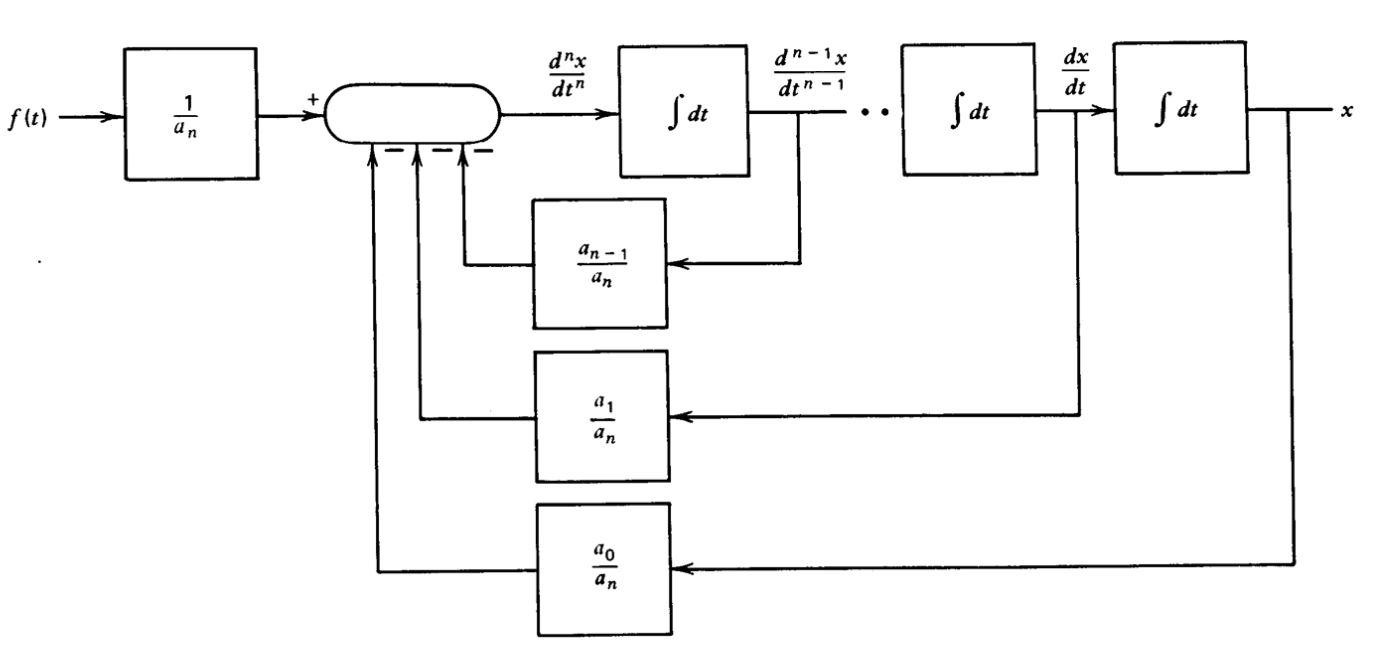
Figure 12.12 Block diagram of Eqn \(\ref{eq12.3.2}\)
Equation \(\ref{eq12.3.2}\) can be represented as the block diagram shown in Figure 12.12. In this representation, the variable \(d^n x/dt^n\) appears as the output of a summation point. Inputs to the summation point are scaled multiples of the driving function and the lower-order derivatives of \(x\). The lower-order derivatives are obtained by successive integrations of \(d^nx/dt^n\), with a total of \(n\) integrations required to complete the block diagram.
Note that the only elements included in the block diagram are a multiple- input summation point, inverters to precede some inputs on the summer, gain blocks, and integrators. Since each of these elements can be readily constructed using operational amplifiers and passive components, the block diagram can be implemented using these devices. When the analog realization is excited with a voltage equal to \(f(t)\), voltages equal in value to \(x\) and its derivatives will be available as the outputs of the integrators.
As an example of this process, consider the differential equation
\[\dfrac{d^4 x}{dt^4} + 2.61 \dfrac{d^3 x}{dt^3} + 3.42 \dfrac{d^2 x}{dt^2} + 2.61 \dfrac{dx}{dt} + x = f(t) \nonumber \]
(We recall from Section 3.3.2 that this equation represents a fourth-order Butterworth filter.) Solving for \(d^4 x/dt^4\) yields
\[\dfrac{d^4 x}{dt^4} = - 2.61 \dfrac{d^3 x}{dt^3} - 3.42 \dfrac{d^2 x}{dt^2} - 2.61 \dfrac{dx}{dt} - x + f(t) \nonumber \]
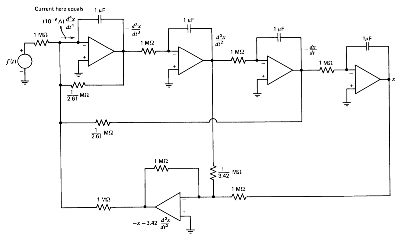
One possible simulation of this equation is shown in Figure 12.13. The voltages expected at the output of various amplifiers are indicated by writing the value of the variable the voltage represents at appropriate nodes. Note that in contrast to traditional analog-computer methods, gains are established by selecting impedances (The relative impedance levels shown in Figure 12.13 are high if general-purpose operational amplifiers such as the LM101A are used. Since only ratios are important in establishing the transfer function, all impedance levels can be scaled to reduce errors that result from amplifier input currents.) used around operational amplifiers rather than by combining potentiometers with fixed-gain amplifiers and integrators. Also, functions have been combined in order to reduce the number of amplifiers required. The use of inverting connections only is traditional in analog computation, and reflects that fact that an operational-amplifier design technique frequently used to improve d-c performance results in an amplifier that can only be used in inverting connections. (See Section 12.3.3.) It may, of course, be possible to use noninverting integrators or summing amplifiers (realized with resistive summing at the input to a noninverting-amplifier connection) if general-purpose operational amplifiers are used for this simulation.
The four integrators appear along the top of the diagram. Since it is assumed that there is no need to have a voltage representing \(d^4 x/dt^4\) available, the summing operation is included in the first integrator connection. The output of this integrator is \(- (d^3x/dt^3)\) when the indicated current is equal to \((10^{-6}\ A) d^4x/dt^4\). Since inverting integrators are used, the signs associated with successive derivatives alternate. The scaling and inversions required by the coefficients of \(x\) and its second derivative are obtained with the bottom amplifier.
The number of amplifiers required in Figure 12.13 indicates the general rule. If this topology is used, simulating an \(n\)th-order linear differential equation requires \(n\) integrators and one amplifier that inverts appropriate signals as necessary to complete feedback paths.
Analog-computing techniques can also be used to solve a variety of non linear differential equations by including hardware that implements the nonlinearity in the simulation. As an example, consider Van der Pol's differential equation
\[\dfrac{d^2 x}{dt^2} + \mu (x^2 - 1) \dfrac{dx}{dt} + x = 0\label{eq12.3.5} \]
where \(\mu\) is a positive constant.
For small values of \(x\), the coefficient of the first derivative term is negative, and increasing-amplitude oscillations result. When the amplitude of the oscillation becomes large enough, the coefficient of the first derivative will be positive over part of the cycle, and a limit cycle can result. Equation \(\ref{eq12.3.5}\) is rewritten in a form convenient for simulation as
\[\dfrac{d^2 x}{dt^2} = -\mu x^2 \dfrac{dx}{dt} + \mu \dfrac{dx}{dt} - x\label{eq12.3.6} \]
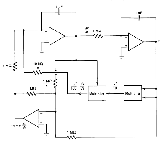
Multipliers are required to generate \(x^2\) and form the \(x^2 (dx/dt)\) product necessary for the simulation of Equation \(\ref{eq12.3.6}\). Two techniques for analog multiplication were described in Sections 11.5.5 and 12.2.2. Practical multi pliers based on these methods are often designed to have an output voltage equal to the product of the two input voltages divided by 10 volts for com patibility with the dynamic range of most solid-state operational amplifiers. Figure 12.14 shows a possible simulation of Equation \(\ref{eq12.3.6}\) assuming that multipliers with this scale factor are used.
Van der Pol's equation is an example of an undriven differential equation, and excitation is by initial conditions only. While initial conditions were not mentioned in our earlier discussion of the simulation of linear differential equations, we recognize that we must specify \(n\) initial conditions in order to determine the complete (homogeneous plus driven) solution of an \(n\)th-order differential equation. These initial conditions can be set simply by establishing the voltages on the integrating capacitors at time \(t = 0\), since these voltages are proportional to the values of \(x\) and its first \(n - 1\) derivatives. A circuit for setting initial conditions is described in Section 12.3.3.
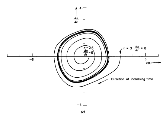
The value of \(x\) as a function of time for Van der Pol's equation with \(\mu = 0.25\) is shown in Figure 12.15. The initial conditions used for parts \(a\) and \(b\) of this figure are \(x(0) = 0.5, (dx/dt)(0) = 0\) and \(x(0) = 3, (dx/dt)(0) = 0\), respectively. We see that in both cases the amplitude of the limit cycle converges to a peak-to-peak value of approximately 4. Part \(c\) of this figure is a plot of \(dx/dt\) versus \(x(t)\). This representation, in which time is a parameter along the curve, is called a phase-plane plot. The responses for both values of initial conditions are included. The convergence to equal-amplitude limit-cycles for both sets of initial conditions is evident in this figure.
The formal procedure described here is certainly not the only one which results in a correct analog representation of a problem. While it does lead to a compact realization, other realizations may maintain better correspondence with the physical system that is being modeled. One popular alternative technique involves simply drawing a block diagram for the system under study, and then implementing the block diagram on a block-by-block basis without ever writing down the complete system differential equation. While this approach often requires more hardware to complete the simulation, it is convenient in that voltages proportional to the actual variables of interest in the problem under study are avaliable. Furthermore, it is generally possible using this alternative to associate scale factors with the parameters of physical elements in the simulated systems on a one-to-one basis.
Amplitude and Time Scaling
Practical considerations constrain the amplitude and frequency range of the signals that arise in analog computation. We normally prefer maximum signal levels that are comfortably below amplifier saturation levels, but well above noise and offset uncertainties. Similarly, very low-frequency signals are difficult to integrate accurately, while the limited gain of an operational amplifier at high frequencies compromises accuracy in this frequency range. Amplitude scaling and time scaling are used to standardize signals to convenient amplitude levels and spectral content.
Amplitude scaling involves little more than some additional bookkeeping effort. Since we are using voltages for all of the dependent variables in our simulation, there must be a dimensioned scale factor that relates the machine variables to the problem variables when the problem variables are quantities other than voltages. For example, if \(x\) is a displacement in meters and some voltage in a simulation represents this variable on a 1 meter = 1 volt basis, the machine variable should really be labeled (1 volt/meter)\(x\) rather than simply \(x\) as is frequently done. We should realize that the number associated with the scale factor can readily be selected to be other than unity. Thus we might use \(10x\) as the label for some voltage, or, preferably (10 volts/meter)\(x\). If this voltage were 7 volts, the corresponding displacement would be \(x\) = (7 volts) (1 meter/ 10 volts) = 0.7 meter. The appropriate values for scale factors can only be determined with a knowledge of approximate problem-variable levels, since the corresponding machine variables should have peak values slightly below the saturation level. Once scale factors have been selected, they are implemented by modifying the gains of amplifiers and integrators from their initially selected values.
Time scaling has advantages beyond those of centering signal-frequency components within the range of optimum operational-amplifier performance. Consider, for example, the simulation of a planetary motion problem that may require years of "real time" to complete. Using a faster "machine time" scale permits us to obtain the solution in a more reasonable time interval. Similarly, the use of a slower than real time scaling procedure allows us to display the buildup of charge in the base region of a transistor at a rate comfortable for viewing on a display oscilloscope.
The technique used for time scaling involves the substitution
\[t = \sigma \tau \label{eq12.3.7} \]
where \(\tau\) is machine time and is equal to real time divided by a scale factor \(\sigma\). A value of a-greater than one implies that the machine solution is faster than the actual solution so that one second of real time is represented by a shorter period \(\tau\) of machine time.
This process is illustrated using the form for a differential equation given in Equation \(\ref{eq12.3.1}\) and repeated here for convenience.
\[a_n \dfrac{d^n x}{dt^n} + a_{n - 1} \dfrac{d^{n - 1} x}{dt^{n - 1}} + \cdots + a_1 \dfrac{dx}{dt} + a_0 x = f(t) \nonumber \]
In order to apply the substitution of Equation \(\ref{eq12.3.7}\), we change \(f(t)\) to \(f(\sigma \tau)\) and change \(d^m x/dt^m\) to \((1/\sigma^m)(d^m x/d\tau^m)\). Thus the time-scaled version of Equation \(\ref{eq12.3.1}\) is
\[\dfrac{a_n}{\sigma^n} \dfrac{d^n x}{d\tau^n} + \dfrac{a_{n-1}}{\sigma^{n - 1}} \dfrac{d^{n - 1} x}{d\tau^{n - 1}} + \cdots + \dfrac{a_1}{\sigma} \dfrac{dx}{d\tau} + a_0 x = f(\sigma \tau) \nonumber \]
The equation when simulated will have a solution identical in form to that of Equation \(\ref{eq12.3.1}\), but will run a factor of a-faster than the original equation.
A second way to implement time scaling is to realize that the dynamics of the simulation are implemented by means of integrations, and that changing the scale factor of every integrator in the simulation by some factor must change the time scale of the simulation by precisely the same factor. Thus problems can be time scaled by first simulating the problem for a real-time solution and then dividing the value of every capacitor by a factor of \(\sigma\). Alternatively, every resistor used to implement all integrators can be reduced in value by a factor of \(\sigma\), or the scale-factor change can be apportioned between resistors and capacitors. The net result of any of these modifications will be to make the problem on the machine run a factor of \(\sigma\) faster than the real-time solution. It is, of course, still necessary to increase the speed of driving functions applied to the system by a factor of \(\sigma\) if these signals are derived from sources that are not implemented using scaled integrators.
The coefficients of the original differential equation often can be used to determine the time scale appropriate to a particular problem. If the roots of the characteristic equation have approximately equal magnitudes, the natural frequencies of the undriven solution will be the order of
\[\omega = \left (\dfrac{a_0}{a_n} \right )^{1/n}\label{eq12.3.9} \]
Conversely, if the system is dominated by one pole, the characteristic frequency is the order of
\[\omega = \dfrac{a_0}{a_1}\label{eq12.3.10} \]
The characteristic frequencies given by Equation \(\ref{eq12.3.9}\) or \(\ref{eq12.3.10}\) can be changed to values convenient for display and compatible with operational-amplifier performance by appropriate selection of \(\sigma\).
The element values that occur in a problem simulation often provide clear indications of the need to modify amplitude or time scales. If, for example, we find that high gain is required at the input of every amplifier being supplied with some particular signal, the scale factor of that signal is probably too small relative to other amplitude scale factors used. Similarly, if one input resistor to a summing amplifier or an integrator is much larger than all other input resistors associated with the amplifier, the implication is that the term applied to the input in question contributes little to the output of the summer or integrator. In the case of time-scale selection, an inappropriate choice is usually reflected by unreasonable resistor values, capacitor values, or both associated with integrators.
The Van der Pol equation simulated earlier (Eqn \(\ref{eq12.3.5}\)) is used as a simple example of time and amplitude scaling. For the range of initial conditions used previously and with \(\mu = 0.25\), the maximum magnitudes of \(x\) and \(dx/dt\) are approximately 3 and \(3\text{ sec}^{-1}\), respectively, while the maximum magnitude of \(d^2 x/dt^2\) is slightly greater than \(3\text{ sec}^{-2}\). Accordingly, if 10-volt maximum amplifier outputs are assumed, scale factors of 3 volts per unit for \(x\) and \(dx/dt\), combined with a scale factor of 2 volts per unit for \(d^2x/dt^2\) are reasonable. If Equation \(\ref{eq12.3.6}\) is rewritten using these scale factors, we obtain
\[2 \dfrac{d^2 x}{dt^2} = -\dfrac{2}{27} \mu (3x)^2 \left (3 \dfrac{dx}{dt} \right ) + \dfrac{2}{3} \mu \left (3 \dfrac{dx}{dt} \right ) - \dfrac{2}{3} (3x) \label{eq12.3.11} \]
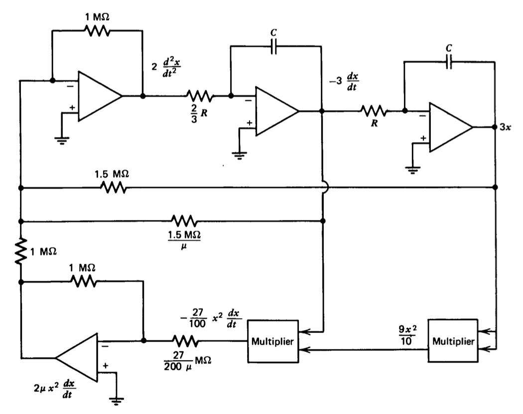
The simulation diagram, again assuming that multipliers with outputs equal to the product of the inputs divided by 10 are used, is shown in Figure 12.16. It has also been assumed in forming this diagram that a voltage proportional to \(d^2x/dt^2\) is required. Note that the input signals applied to the first amplifier are negatives of the right-hand side of Equation \(\ref{eq12.3.11}\) because of the inversion associated with this amplifier. The transfer function of the first integrator is \(-(3/2s)\) so that it provides an output of \(-3(dx/dt)\) when driven with \(2(d^2x/dt^2)\). Alternate scaling may be advan tageous if different values of \(\mu\) are used to keep the maximum magnitudes of the voltages proportional to \(dx/dt\) and \(d^2 x/dt^2\) at optimum levels.
If a value of \(RC = 1\) second is used, the solution will run at real time, and the oscillation frequency will be about one radian per second. Changing this product will time scale the solution. For example, the use of \(RC = 1\) ms results in limit-cycle oscillation at approximately 1000 radians per second.
Ancillary Circuits
There are several interesting circuit configurations that are frequently employed in analog computation and that also can be used in other more general applications.
One of these topologies is the three-mode integrator. We have seen that it is necessary to apply initial conditions to integrators in order to obtain complete (homogeneous plus driven) solutions for simulated differential equations. Another useful computing mode results if all integrators are simultaneously switched to a state where their outputs become time in variant and thus hold the values that were present at the switching time. The values of problem variables at the switching time can then be deter mined accurately with a digital voltmeter.
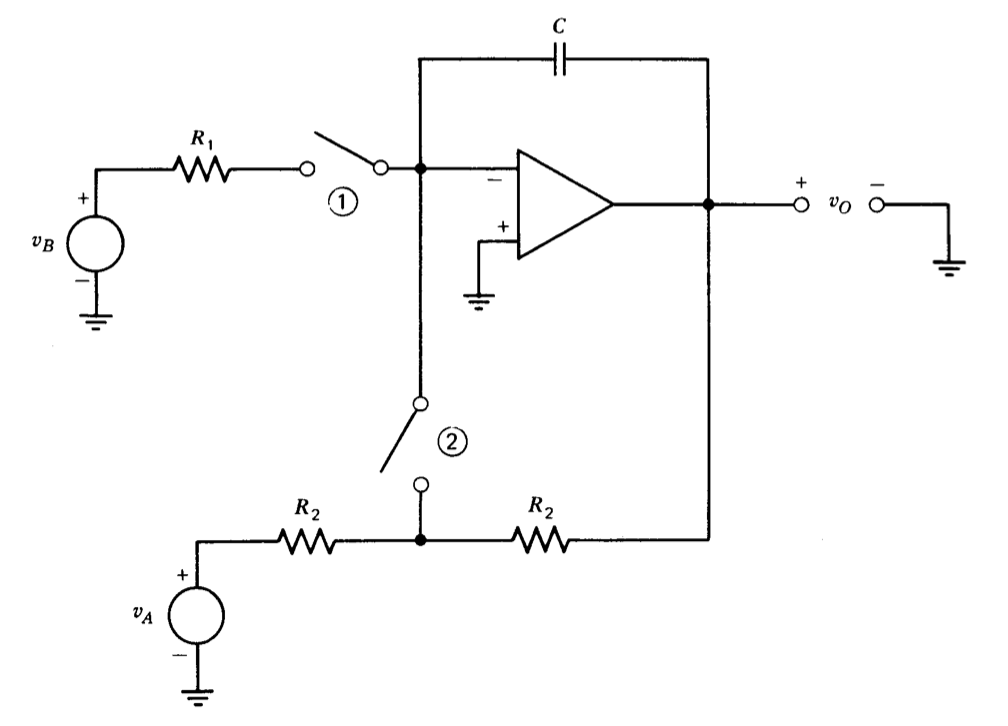
The three-mode integrator shown in Figure 12.17 permits application of initial conditions and allows holding an output voltage in addition to functioning as an integrator. The reset (or initial condition), operate, and hold modes are selected by appropriate choice of switch positions. With switch ① open and switch ② closed, the amplifier closed-loop transfer function is
\[\dfrac{V_o (s)}{V_a (s)} = -\dfrac{1}{R_2 Cs + 1} \nonumber \]
If \(v_A\) is time invariant in this mode, the capacitor will charge so that the output voltage eventually becomes the negative of \(v_A\). The capacitor voltage can then provide initial conditions for subsequent operations.
If switch ① is closed and switch ② is open, the amplifier integrates \(v_B\) in the usual fashion.
With both switches open, capacitor current is limited to operational-amplifier input current and capacitor self-leakage; thus capacitor voltage is ideally time invariant.
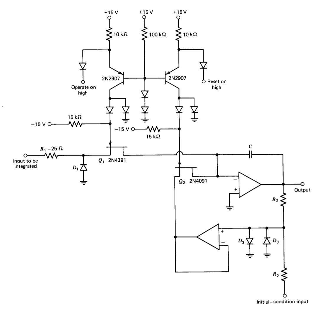
The required reset time of the connection shown in Figure 12.17 can be quite long if reasonable values are used for the resistors labeled \(R_2\). The use of a second operational amplifier connected as a voltage follower and supplying a low-resistance drive for the inverting input of the integrator can substantially shorten reset times. A practical three-mode integrator circuit that incorporates this feature is shown in Figure 12.18.
The bipolar-transistor drivers are compatible with \(T^2 L\) logic signals, and drive the gate potential of field-effect-transistor switches to ground on inputs that exceed two diode forward voltages. With a high level for the "operate" signal and the "reset" signal at ground, \(Q_1\) is on and \(Q_2\) is off. This combination puts the circuit in the normal integrating mode. FET \(Q_1\) has a drain-to-source on resistance of approximately 25 ohms, and this value is compensated for by reducing the integrating-resistor size by a
corresponding amount. Diode \(D_1\) does not conduct significant current in this state. Diodes \(D_2\) and \(D_3\) keep the output of the follower within approximately 0.6 volt of ground. One benefit of this clamping is that the source of \(Q_2\) cannot become negative enough to initiate conduction with its gate at - 15 volts, since the maximum pinchoff voltage of the 2N4391 is 10 volts. Clamping the follower input level also keeps its signal levels near those anticipated during reset thus avoiding long slewing periods when the circuit is switched to apply initial conditions.
With the gate of \(Q_1\) at - 15 volts (corresponding to a low level on the "operate" control line), diode \(D_1\) prevents source potentials that would initiate conduction of transistor \(Q_1\). If \(Q_2\) is on, the output voltage is driven toward the negative of the initial-condition input-signal level. The details of the transient for a large error depend on diode, FET, and amplifier characteristics. As the error signal becomes smaller, the reset loop enters its linear operating region. The reader should convince himself that the linear-region transmission of the reset loop (assuming ideal operational amplifiers) is \(-1/2r_{ds} Cs\), where \(r_{ds}\), is the incremental drain-to-source on resistance of the FET. Thus the low FET resistance, rather than \(R_2\), determines linear-region dynamics.
The hold mode results with both the "operate" and the "reset" signals at ground so that both FET's are off. In this state the current supplied to the capacitor is determined by FET leakage and amplifier input current.
One application for this type of circuit in addition to its use in analog computation is as a sample-and-hold circuit. In this case the operate switch is not needed, and the circuit is switched from sampling the negative of an input voltage to hold with \(Q_2\).
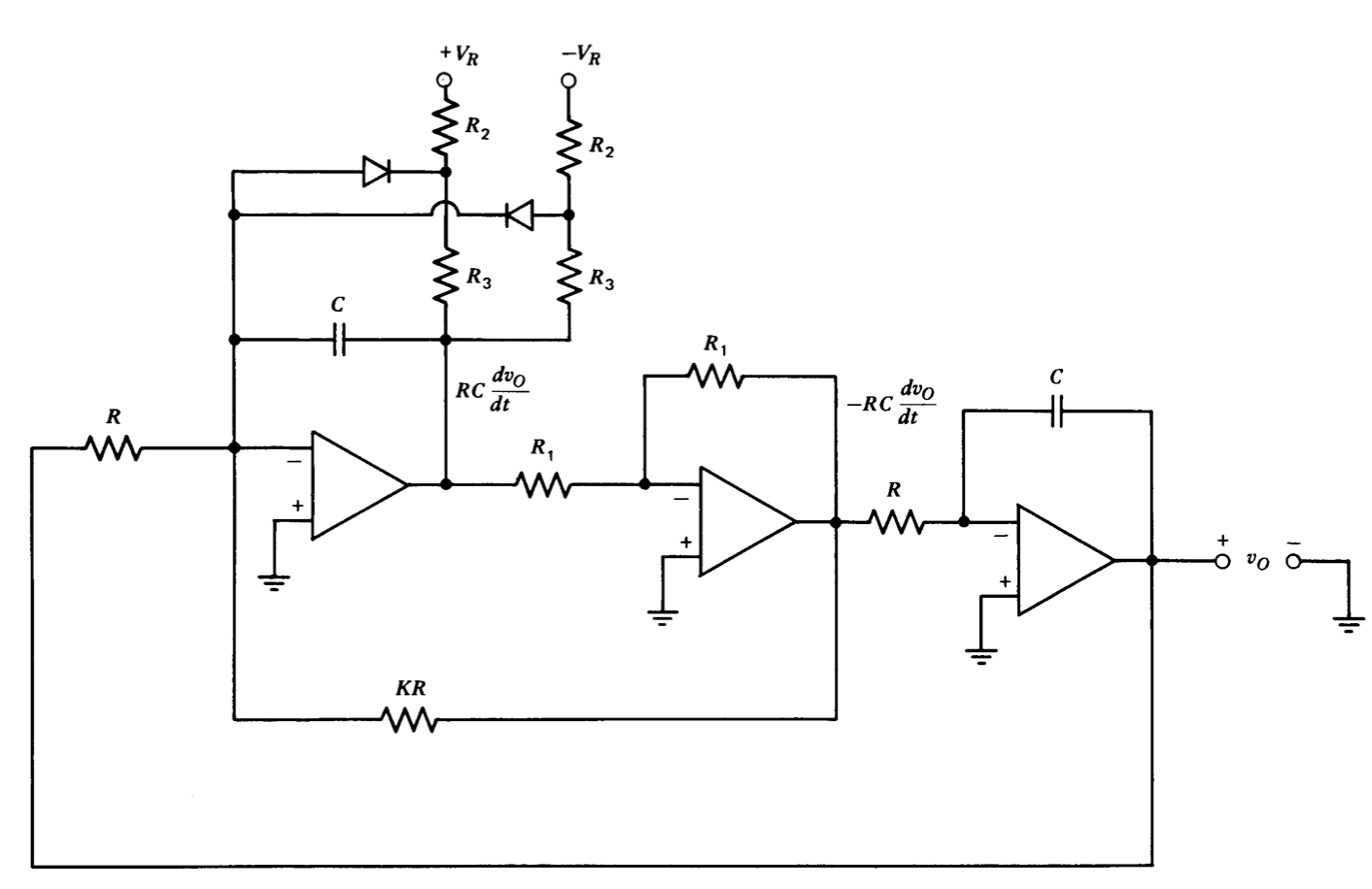
Sinusoidal signals are frequently used as test inputs in analog-computer simulations. A quadrature oscillator that includes limiting and that is easily assembled using components available on most analog computers is shown in Figure 12.19. The diagram implies a simulated differential equation, prior to limiting, of
\[-R^2 C^2 \dfrac{d^2 v_O}{dt^2} = -\dfrac{RC}{K} \dfrac{dv_O}{dt} + v_O \nonumber \]
We recognize this equation as a linear, second-order differential equation with \(\omega_n = 1/RC\) and \(\zeta = - 1/2K\). The value of \(K\) is chosen small enough to guarantee oscillation with anticipated capacitor losses and amplifier imperfections, thus insuring that signal amplitudes will be determined primarily by the diode-resistor networks shown.
A precisely known voltage reference is required in many simulations to apply constant input signals, provide initial-condition voltages, function .as a bias level for nonlinearities, or for other purposes. Voltage references are also used regularly in a host of applications unrelated to analog simulation.
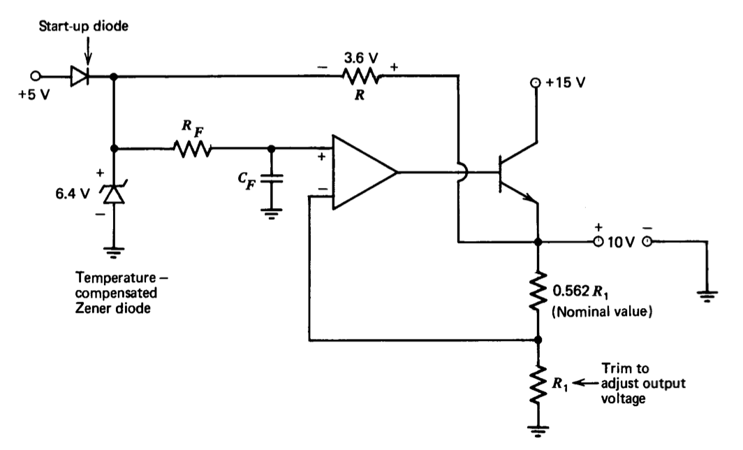
The circuit shown in Figure 12.20 is a simple yet highly stable voltage refer ence. The operational amplifier is connected for a noninverting gain of slightly more than 1.5 so that a 10-volt output results with 6.4 volts applied to the noninverting amplifier input.
With the topology as shown, the voltage across the resistor connected from the amplifier output to its noninverting input is constrained by the amplifier closed-loop gain to be 0.562 \(V_Z\) where \(V_Z\) is the forward voltage of the Zener diode. The current through this resister is the bias current applied to the Zener diode. Zener-diode current is thus established by the stable value of the Zener voltage itself. The Zener output resistance does not deteriorate voltage regulation since the diode is operated at constant current in this connection. The filter following the Zener diode helps to attentuate noise fluctuations in its output voltage.
An emitter follower is included inside the operational-amplifier loop to increase output current capacity (current limiting circuitry as discussed in Section 8.4 is often a worthwhile precaution) and to lower output impedance, particularly at higher frequencies. While the low-frequency output impedance of the circuit would be small even without the follower because of feedback, this impedance would increase to the amplifier open-loop output impedance at frequencies above crossover. The emitter follower reduces open-loop output impedance to improve performance when pulsed or high-frequency load-current changes are anticipated. A shunt capacitor at the output may also be used to lower high-frequency output impedance. (See Section 5.2.2.)
The bootstrapping used to excite the Zener diode is of course a form of positive feedback and would deteriorate performance if the magnitude of this feedback approached unity. The low-frequency transmission of the positive feedback loop is
\[L = 1.562 \dfrac{r_d}{R + r_d} \label{eq12.3.14} \]
where \(r_d\) is the incremental resistance of the Zener diode. This expression is evaluated using parameters for a 1N829A, a temperature-compensated Zener diode. The diode is designed for an operating current of \(7.5\ mA\), and thus \(R\) will be approximately 500 \(\Omega\). The incremental resistance of the diode is specified as a maximum of 10 \(\Omega\). Thus the loop transmission is, from Equation \(\ref{eq12.3.14}\), 0.03. This small amount of positive feedback does not significantly affect performance.
The positive feedback can result in the circuit operating with the diode in its forward-conducting state rather than its normal reverse-breakdown mode. This state, which leads to a negative output of approximately one volt, can be eliminated with the start-up diode shown. The start-up diode insures that the Zener diode is forced into its reverse region, but does not contribute to Zener current under normal operating conditions.
The expected operational-amplifier imperfections have relatively little effect on the overall performance of the reference circuit. A value of 30,000 for supply-voltage rejection ratio (typical for integrated-circuit amplifiers) causes a change in output voltage of approximately 50 AV per volt of supply change. (This \(33\ \mu V/V\) sensitivity is amplified by the closed-loop gain of 1.5.) The typical input-voltage drift for many inexpensive operational amplifiers is the order of \(5\ \mu V\) per degree Centigrade. This figure is not significant compared to the temperature coefficient of 5 parts per million per degree Centigrade or approximately \(32\ \mu V\) per degree Centigrade of a high-quality Zener diode such as the 1N829A.
The designers of the large analog computers that evolved during the period from the early 1950s to the mid-1960s often devoted almost fanatical
effort to achieving high static accuracy in their computing elements. Toward this end, operational amplifiers were surrounded with high-precision wire- wound resistors and capacitors that could be accurately trimmed to desired values. These passive components were often placed in temperature-stable ovens to eliminate variations with ambient temperature.
The low-frequency errors (particularly input voltage offset) characteristic of vacuum-tube operational amplifiers were largely eliminated by means of an imaginative technique known as chopper stabilization.(E. A. Goldberg, "Stabilization of Wide-Band Direct Current Amplifiers for Zero and Gain," RCA Review, Vol. II, No. 2, June 1950, pp. 296-300. ) This method
is still incorporated into some modern operational-amplifier designs, and it provides a way of reducing the voltage drift and input current of an amplifier to vanishingly small levels. The usual implementation of this technique can be viewed as an extreme example of feedforward (see Section 8.2.2) and thus results in an amplifier that can only be used in inverting connections.
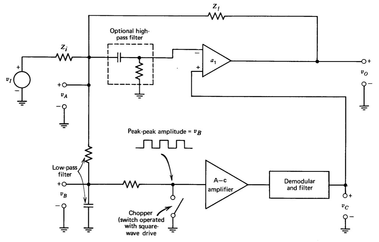
Figure 12.21 illustrates the concept. Assume that the optional network is eliminated so that the junction of \(Z_f\) and \(Z_i\) is connected directly to the inverting input of the top amplifier. The resulting connection clearly functions as an inverting amplifier if the voltage \(v_C\) is zero. Observe that one necessary condition for the amplifier closed-loop gain to be equal to its ideal value is that \(v_A = 0\). The objective of chopper stabilization is to reduce \(v_A\) to nearly zero by applying an appropriate signal to the non- inverting input of the top amplifier.
The d-c component of the voltage \(v_A\) is determined with a low-pass filter, and this component (\(v_B\)) is "chopped" (converted to a square wave with peak-to-peak amplitude \(v_B\)) using a periodically operated switch. (Early designs used vibrating-reed mechanical switches, while more modern units often use periodically illuminated photoresistors or field-effect transistors as the switch.) The chopped a-c signal can be amplified without offset by an a-c amplifier and demodulated to produce a signal \(v_C\) proportional to \(v_B\). If the gain of the a-c amplifier is high, the low-frequency gain \(v_C/v_A = a_{02}\) will be high. If \(a_{02}\) is negative, the signal applied to the positive gain input of the top amplifier will be of the correct polarity to drive \(v_A\) toward zero. Arbitrarily small d-c components of \(v_A\) can theoretically be obtained by having a sufficiently high magnitude for \(a_{02}\), although in practice achievable offsets are limited by errors such as thermally induced voltages in the switch itself. The low-pass filter is necessary to prevent sampling errors that arise if signals in excess of half the chopping frequency are applied to the chopper.
An alternative way to view the operation of a chopper-stabilized amplifier is to notice that high-frequency signals pass directly through the top amplifier, while components below the cutoff frequency of the low-pass filter are amplified by both the bottom amplifier and the top amplifier in cascade. (It is interesting to observe that low-frequency open-loop gain magnitudes in excess of 10 have been achieved in this way.) It is therefore not necessary to apply low-frequency signals directly to the top amplifier, and a high-pass filter (shown as the optional network) can be included in series with the inverting input of the top amplifier. As a result, both voltage offset and input current to the operational amplifier can be reduced by chopper stabilization, yielding an amplifier with virtually ideal low-frequency characteristics.
Several manufacturers offer packages that combine discrete-component choppers with integrated-circuit amplifiers. More recently, integrated circuit manufacturers have been able to fabricate complete chopper- stabilized amplifiers either in monolothic form or by combining several monolithic chips to form a hybrid circuit. These circuits incorporate topological improvements that permit true differential operation. The large capacitors required are connected externally to the package. Drifts of a fraction of a microvolt per degree Centigrade, coupled with input currents in the picoampere range, are available at surprisingly low cost.