
5.10: Problems
- Page ID
- 28558

\( \newcommand{\vecs}[1]{\overset { \scriptstyle \rightharpoonup} {\mathbf{#1}} } \)
\( \newcommand{\vecd}[1]{\overset{-\!-\!\rightharpoonup}{\vphantom{a}\smash {#1}}} \)
\( \newcommand{\id}{\mathrm{id}}\) \( \newcommand{\Span}{\mathrm{span}}\)
( \newcommand{\kernel}{\mathrm{null}\,}\) \( \newcommand{\range}{\mathrm{range}\,}\)
\( \newcommand{\RealPart}{\mathrm{Re}}\) \( \newcommand{\ImaginaryPart}{\mathrm{Im}}\)
\( \newcommand{\Argument}{\mathrm{Arg}}\) \( \newcommand{\norm}[1]{\| #1 \|}\)
\( \newcommand{\inner}[2]{\langle #1, #2 \rangle}\)
\( \newcommand{\Span}{\mathrm{span}}\)
\( \newcommand{\id}{\mathrm{id}}\)
\( \newcommand{\Span}{\mathrm{span}}\)
\( \newcommand{\kernel}{\mathrm{null}\,}\)
\( \newcommand{\range}{\mathrm{range}\,}\)
\( \newcommand{\RealPart}{\mathrm{Re}}\)
\( \newcommand{\ImaginaryPart}{\mathrm{Im}}\)
\( \newcommand{\Argument}{\mathrm{Arg}}\)
\( \newcommand{\norm}[1]{\| #1 \|}\)
\( \newcommand{\inner}[2]{\langle #1, #2 \rangle}\)
\( \newcommand{\Span}{\mathrm{span}}\) \( \newcommand{\AA}{\unicode[.8,0]{x212B}}\)
\( \newcommand{\vectorA}[1]{\vec{#1}} % arrow\)
\( \newcommand{\vectorAt}[1]{\vec{\text{#1}}} % arrow\)
\( \newcommand{\vectorB}[1]{\overset { \scriptstyle \rightharpoonup} {\mathbf{#1}} } \)
\( \newcommand{\vectorC}[1]{\textbf{#1}} \)
\( \newcommand{\vectorD}[1]{\overrightarrow{#1}} \)
\( \newcommand{\vectorDt}[1]{\overrightarrow{\text{#1}}} \)
\( \newcommand{\vectE}[1]{\overset{-\!-\!\rightharpoonup}{\vphantom{a}\smash{\mathbf {#1}}}} \)
\( \newcommand{\vecs}[1]{\overset { \scriptstyle \rightharpoonup} {\mathbf{#1}} } \)
\( \newcommand{\vecd}[1]{\overset{-\!-\!\rightharpoonup}{\vphantom{a}\smash {#1}}} \)
\(\newcommand{\avec}{\mathbf a}\) \(\newcommand{\bvec}{\mathbf b}\) \(\newcommand{\cvec}{\mathbf c}\) \(\newcommand{\dvec}{\mathbf d}\) \(\newcommand{\dtil}{\widetilde{\mathbf d}}\) \(\newcommand{\evec}{\mathbf e}\) \(\newcommand{\fvec}{\mathbf f}\) \(\newcommand{\nvec}{\mathbf n}\) \(\newcommand{\pvec}{\mathbf p}\) \(\newcommand{\qvec}{\mathbf q}\) \(\newcommand{\svec}{\mathbf s}\) \(\newcommand{\tvec}{\mathbf t}\) \(\newcommand{\uvec}{\mathbf u}\) \(\newcommand{\vvec}{\mathbf v}\) \(\newcommand{\wvec}{\mathbf w}\) \(\newcommand{\xvec}{\mathbf x}\) \(\newcommand{\yvec}{\mathbf y}\) \(\newcommand{\zvec}{\mathbf z}\) \(\newcommand{\rvec}{\mathbf r}\) \(\newcommand{\mvec}{\mathbf m}\) \(\newcommand{\zerovec}{\mathbf 0}\) \(\newcommand{\onevec}{\mathbf 1}\) \(\newcommand{\real}{\mathbb R}\) \(\newcommand{\twovec}[2]{\left[\begin{array}{r}#1 \\ #2 \end{array}\right]}\) \(\newcommand{\ctwovec}[2]{\left[\begin{array}{c}#1 \\ #2 \end{array}\right]}\) \(\newcommand{\threevec}[3]{\left[\begin{array}{r}#1 \\ #2 \\ #3 \end{array}\right]}\) \(\newcommand{\cthreevec}[3]{\left[\begin{array}{c}#1 \\ #2 \\ #3 \end{array}\right]}\) \(\newcommand{\fourvec}[4]{\left[\begin{array}{r}#1 \\ #2 \\ #3 \\ #4 \end{array}\right]}\) \(\newcommand{\cfourvec}[4]{\left[\begin{array}{c}#1 \\ #2 \\ #3 \\ #4 \end{array}\right]}\) \(\newcommand{\fivevec}[5]{\left[\begin{array}{r}#1 \\ #2 \\ #3 \\ #4 \\ #5 \\ \end{array}\right]}\) \(\newcommand{\cfivevec}[5]{\left[\begin{array}{c}#1 \\ #2 \\ #3 \\ #4 \\ #5 \\ \end{array}\right]}\) \(\newcommand{\mattwo}[4]{\left[\begin{array}{rr}#1 \amp #2 \\ #3 \amp #4 \\ \end{array}\right]}\) \(\newcommand{\laspan}[1]{\text{Span}\{#1\}}\) \(\newcommand{\bcal}{\cal B}\) \(\newcommand{\ccal}{\cal C}\) \(\newcommand{\scal}{\cal S}\) \(\newcommand{\wcal}{\cal W}\) \(\newcommand{\ecal}{\cal E}\) \(\newcommand{\coords}[2]{\left\{#1\right\}_{#2}}\) \(\newcommand{\gray}[1]{\color{gray}{#1}}\) \(\newcommand{\lgray}[1]{\color{lightgray}{#1}}\) \(\newcommand{\rank}{\operatorname{rank}}\) \(\newcommand{\row}{\text{Row}}\) \(\newcommand{\col}{\text{Col}}\) \(\renewcommand{\row}{\text{Row}}\) \(\newcommand{\nul}{\text{Nul}}\) \(\newcommand{\var}{\text{Var}}\) \(\newcommand{\corr}{\text{corr}}\) \(\newcommand{\len}[1]{\left|#1\right|}\) \(\newcommand{\bbar}{\overline{\bvec}}\) \(\newcommand{\bhat}{\widehat{\bvec}}\) \(\newcommand{\bperp}{\bvec^\perp}\) \(\newcommand{\xhat}{\widehat{\xvec}}\) \(\newcommand{\vhat}{\widehat{\vvec}}\) \(\newcommand{\uhat}{\widehat{\uvec}}\) \(\newcommand{\what}{\widehat{\wvec}}\) \(\newcommand{\Sighat}{\widehat{\Sigma}}\) \(\newcommand{\lt}{<}\) \(\newcommand{\gt}{>}\) \(\newcommand{\amp}{&}\) \(\definecolor{fillinmathshade}{gray}{0.9}\)5.10.1: Review Questions
1. Define gain-bandwidth product. What is its use?
2. How do you determine \(f_2\) and \(f_1\) for a multi-stage circuit?
3. What happens if two or more stages share the same break frequency?
4. What is slew rate?
5. How is power bandwidth determined?
6. How do power bandwidth and small-signal bandwidth differ?
7. What are the advantages and disadvantages of noncompensated op amps?
8. What are decompensated op amps?
9. What causes DC offset voltage?
10. What causes DC drift voltage?
11. What is CMRR?
12. What is PSRR?
13. What parameters describe an op amps noise performance?
14. What is S/N?
5.10.2: Problems
Analysis Problems
1. Determine \(f_2\) for the circuit in Figure 5.3.3 if a 411 op amp is used.
2. Determine \(f_2\) for the circuit of Figure 5.3.5 if a 318 op amp is used. Note: \(f_{unity}\) = 15 MHz for a 318.
3. What is the minimum acceptable \(f_{unity}\) for the op amp in Figure 5.3.3 if the desired \(f_2\) is 250 kHz?
4. What is the minimum acceptable \(f_{unity}\) for the op amp in Figure 5.3.5 if the desired \(f_2\) is 20 kHz?
5. Determine the power bandwidth for Problem 5.1. Assume \(V_p\) = 10 V.
6. Determine the power bandwidth for Problem 5.3. Assume \(V_p\) = 12 V.
7. What is the minimum acceptable slew rate for the circuit of Figure 5.3.3 if the desired power bandwidth is 20 kHz with a \(V_p\) of 10 V?
8. What is the minimum acceptable slew rate for the circuit of Figure 5.3.5 if the desired power bandwidth is 40 kHz with a \(V_p\) of 5 V?
9. A circuit has the following specifications: \(\pm\)15 V power supply, voltage gain equals 26 dB, desired power bandwidth equals 80 kHz at clipping. Determine the minimum acceptable slew rate for the op amp.
10. Determine the system \(f_2\) in Figure 5.3.6 if all three devices are 318s.
11. Determine the system slew rate for Figure 5.3.7. The first device is a 741 and the second unit is a 411.
12. Find the output offset voltage for Figure 5.3.3.
13. If \(R_s = R_f = 100 \Omega \) in Figure 5.5.2, find the output offset voltage using a 318 op amp.
14. Assume that the circuit of Figure 5.5.3 is nulled at 25\(^{\circ}\)C and that an optimum value for \(R_{off}\) is used. Determine the drift at 75\(^{\circ}\)C.
15. Assuming that the 120 Hz power supply ripple in Figure \(\PageIndex{1}\) is 50 mV, how large is its contribution to the output?
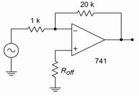
Figure \(\PageIndex{1}\)
16. Utilizing a 5534 op amp, what is the approximate input noise voltage for a source resistance of 1 k\(\Omega \) and a bandwidth from 10 Hz to 20 kHz?
17. Assuming that the op amp of Problem 5.16 is connected like Figure \(\PageIndex{1}\), what is the approximate output noise voltage? What is the approximate input referred noise voltage?
18. Assume that \(R_s = 0 \Omega \), \(R_i = 500 \Omega \), and \(R_f = 10 k\Omega \) in Figure 5.8.2. Find the input noise voltage if the op amp is a 411.
19. For a nominal output voltage of 2 V RMS, determine the signal-to-noise ratio for Problem 5.18. Assume that the input to Figure 5.5.2 is a 5 V peak 50 kHz square wave. Draw the output waveform if a 741 is used.
21. Repeat Problem 5.20 using a 10 V peak, 100 kHz sine wave.
Design Problems
22. Determine an optimum value for \(R_{off}\) in Figure 5.3.3 and determine the resulting offset voltage.
23. Determine the optimum value for \(R_{off}\) in Figure \(\PageIndex{1}\). Assuming that the circuit has been nulled at 25\(^{\circ}\)C, find the drift at 60\(^{\circ}\)C.
24. Determine a new value for the 100 k\(\Omega \) resistor in Figure 5.3.8 in order to minimize the output offset.
25. Using the optimum resistor found in Problem 5.24, determine a new value for the input capacitor that will maintain the original \(f_1\).
26. Design a circuit with a gain of 32 dB and an \(f_2\) of at least 100 kHz. You may use any of the following: 741, 411, 318.
27. Design a circuit with a gain of 50 and an \(f_{max}\) of at least 50 kHz, given a maximum output swing of 10 V peak. You may use any of the following: 741, 411, 318.
28. Design a circuit with a gain of 12 dB, a small-signal bandwidth of at least 100 kHz, and an \(f_{max}\) of at least 100 kHz for a peak output swing of 12 V.
29. Utilizing two or more stages, design a circuit with a gain of 150 and a small signal bandwidth of at least 600 kHz.
Challenge Problems
30. Determine the system \(f_2\) in Figure 5.4.10.
31. Determine the input noise voltage for the circuit of Figure \(\PageIndex{1}\). Assume \(R_{off}\) = 950 \(\Omega \).
32. Determine the output noise voltage and the input-referred noise voltage for Problem 5.31.
33. Assuming that driving source resistance in Figure 5.3.7 is 0 \(\Omega \), how much offset voltage is produced at the output of the circuit? Assume that both devices are 411's.
34. Assume that you have one each of: 411, 741, 318. Determine the combination that will yield the highest system slew rate in Figure \(\PageIndex{2}\).
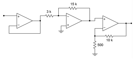
Figure \(\PageIndex{2}\)
35. Repeat Problem 5.34 in order to produce the highest system \(f_2\).
36. Assuming that the driving source resistance is 0 \(\Omega \) in Figure 5.3.7. Determine the output noise voltage if both devices are 411's.
37. Derive Equation 5.3.9 from the text.
Computer Simulation Problems
38. Use a simulator to create a Bode plot for Problem 5.10. If a macro model for the LM318 is not available, use the 741 instead.
39. Create a time domain representation of the output voltage of Problem 5.20 using a simulator.
40. Create a time domain representation of the output voltage of Problem 5.21 using a simulator. Repeat the simulation using an LM318 op amp in place of the 741. What do the results indicate?
41. Simulate the circuit designed in Problem 5.26. Verify \(f_2\) and \(A_v\) through a Bode plot.
42. Generate a Bode plot using a simulator and verify \(f_2\) and \(A_v\) for the circuit designed in Problem 5.29.
43. Generate a Bode plot using a simulator and verify \(f_2\) for the circuit designed in Problem 5.35.