
12.4: Digital-to-Analog Conversion Techniques
- Page ID
- 3624

\( \newcommand{\vecs}[1]{\overset { \scriptstyle \rightharpoonup} {\mathbf{#1}} } \)
\( \newcommand{\vecd}[1]{\overset{-\!-\!\rightharpoonup}{\vphantom{a}\smash {#1}}} \)
\( \newcommand{\id}{\mathrm{id}}\) \( \newcommand{\Span}{\mathrm{span}}\)
( \newcommand{\kernel}{\mathrm{null}\,}\) \( \newcommand{\range}{\mathrm{range}\,}\)
\( \newcommand{\RealPart}{\mathrm{Re}}\) \( \newcommand{\ImaginaryPart}{\mathrm{Im}}\)
\( \newcommand{\Argument}{\mathrm{Arg}}\) \( \newcommand{\norm}[1]{\| #1 \|}\)
\( \newcommand{\inner}[2]{\langle #1, #2 \rangle}\)
\( \newcommand{\Span}{\mathrm{span}}\)
\( \newcommand{\id}{\mathrm{id}}\)
\( \newcommand{\Span}{\mathrm{span}}\)
\( \newcommand{\kernel}{\mathrm{null}\,}\)
\( \newcommand{\range}{\mathrm{range}\,}\)
\( \newcommand{\RealPart}{\mathrm{Re}}\)
\( \newcommand{\ImaginaryPart}{\mathrm{Im}}\)
\( \newcommand{\Argument}{\mathrm{Arg}}\)
\( \newcommand{\norm}[1]{\| #1 \|}\)
\( \newcommand{\inner}[2]{\langle #1, #2 \rangle}\)
\( \newcommand{\Span}{\mathrm{span}}\) \( \newcommand{\AA}{\unicode[.8,0]{x212B}}\)
\( \newcommand{\vectorA}[1]{\vec{#1}} % arrow\)
\( \newcommand{\vectorAt}[1]{\vec{\text{#1}}} % arrow\)
\( \newcommand{\vectorB}[1]{\overset { \scriptstyle \rightharpoonup} {\mathbf{#1}} } \)
\( \newcommand{\vectorC}[1]{\textbf{#1}} \)
\( \newcommand{\vectorD}[1]{\overrightarrow{#1}} \)
\( \newcommand{\vectorDt}[1]{\overrightarrow{\text{#1}}} \)
\( \newcommand{\vectE}[1]{\overset{-\!-\!\rightharpoonup}{\vphantom{a}\smash{\mathbf {#1}}}} \)
\( \newcommand{\vecs}[1]{\overset { \scriptstyle \rightharpoonup} {\mathbf{#1}} } \)
\( \newcommand{\vecd}[1]{\overset{-\!-\!\rightharpoonup}{\vphantom{a}\smash {#1}}} \)
\(\newcommand{\avec}{\mathbf a}\) \(\newcommand{\bvec}{\mathbf b}\) \(\newcommand{\cvec}{\mathbf c}\) \(\newcommand{\dvec}{\mathbf d}\) \(\newcommand{\dtil}{\widetilde{\mathbf d}}\) \(\newcommand{\evec}{\mathbf e}\) \(\newcommand{\fvec}{\mathbf f}\) \(\newcommand{\nvec}{\mathbf n}\) \(\newcommand{\pvec}{\mathbf p}\) \(\newcommand{\qvec}{\mathbf q}\) \(\newcommand{\svec}{\mathbf s}\) \(\newcommand{\tvec}{\mathbf t}\) \(\newcommand{\uvec}{\mathbf u}\) \(\newcommand{\vvec}{\mathbf v}\) \(\newcommand{\wvec}{\mathbf w}\) \(\newcommand{\xvec}{\mathbf x}\) \(\newcommand{\yvec}{\mathbf y}\) \(\newcommand{\zvec}{\mathbf z}\) \(\newcommand{\rvec}{\mathbf r}\) \(\newcommand{\mvec}{\mathbf m}\) \(\newcommand{\zerovec}{\mathbf 0}\) \(\newcommand{\onevec}{\mathbf 1}\) \(\newcommand{\real}{\mathbb R}\) \(\newcommand{\twovec}[2]{\left[\begin{array}{r}#1 \\ #2 \end{array}\right]}\) \(\newcommand{\ctwovec}[2]{\left[\begin{array}{c}#1 \\ #2 \end{array}\right]}\) \(\newcommand{\threevec}[3]{\left[\begin{array}{r}#1 \\ #2 \\ #3 \end{array}\right]}\) \(\newcommand{\cthreevec}[3]{\left[\begin{array}{c}#1 \\ #2 \\ #3 \end{array}\right]}\) \(\newcommand{\fourvec}[4]{\left[\begin{array}{r}#1 \\ #2 \\ #3 \\ #4 \end{array}\right]}\) \(\newcommand{\cfourvec}[4]{\left[\begin{array}{c}#1 \\ #2 \\ #3 \\ #4 \end{array}\right]}\) \(\newcommand{\fivevec}[5]{\left[\begin{array}{r}#1 \\ #2 \\ #3 \\ #4 \\ #5 \\ \end{array}\right]}\) \(\newcommand{\cfivevec}[5]{\left[\begin{array}{c}#1 \\ #2 \\ #3 \\ #4 \\ #5 \\ \end{array}\right]}\) \(\newcommand{\mattwo}[4]{\left[\begin{array}{rr}#1 \amp #2 \\ #3 \amp #4 \\ \end{array}\right]}\) \(\newcommand{\laspan}[1]{\text{Span}\{#1\}}\) \(\newcommand{\bcal}{\cal B}\) \(\newcommand{\ccal}{\cal C}\) \(\newcommand{\scal}{\cal S}\) \(\newcommand{\wcal}{\cal W}\) \(\newcommand{\ecal}{\cal E}\) \(\newcommand{\coords}[2]{\left\{#1\right\}_{#2}}\) \(\newcommand{\gray}[1]{\color{gray}{#1}}\) \(\newcommand{\lgray}[1]{\color{lightgray}{#1}}\) \(\newcommand{\rank}{\operatorname{rank}}\) \(\newcommand{\row}{\text{Row}}\) \(\newcommand{\col}{\text{Col}}\) \(\renewcommand{\row}{\text{Row}}\) \(\newcommand{\nul}{\text{Nul}}\) \(\newcommand{\var}{\text{Var}}\) \(\newcommand{\corr}{\text{corr}}\) \(\newcommand{\len}[1]{\left|#1\right|}\) \(\newcommand{\bbar}{\overline{\bvec}}\) \(\newcommand{\bhat}{\widehat{\bvec}}\) \(\newcommand{\bperp}{\bvec^\perp}\) \(\newcommand{\xhat}{\widehat{\xvec}}\) \(\newcommand{\vhat}{\widehat{\vvec}}\) \(\newcommand{\uhat}{\widehat{\uvec}}\) \(\newcommand{\what}{\widehat{\wvec}}\) \(\newcommand{\Sighat}{\widehat{\Sigma}}\) \(\newcommand{\lt}{<}\) \(\newcommand{\gt}{>}\) \(\newcommand{\amp}{&}\) \(\definecolor{fillinmathshade}{gray}{0.9}\)The basic digital-to-analog converter is little more than a weighted summing amplifier. Each successive bit in the digital word represents a level that is twice as large as the preceding bit. If each bit is taken as a given current or voltage, the increasing levels may be produced by using different gains in the summing inputs. A simple four-bit converter is shown in Figure \(\PageIndex{1}\).
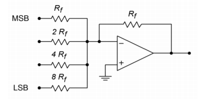
Figure \(\PageIndex{1}\): A simple 4-bit converter.
This system can represent \(2^4\), or 16, different levels. Each input is driven by a simple high/low logic level that represents a 1 or 0 for that particular bit. Note that the input resistors vary by factors of 2. The gain for the upper most path is \(R_f/R_f\), or unity. This input is used for the most significant bit of the input word (MSB). The next input shows a gain of \(R_f / (2R_f)\), or 0.5. The third input shows a gain of 0.25, and the final input shows a gain of 0.125. The final input has the lowest gain and is used for the least significant bit of the input word (LSB). If the input word had a higher resolution (i.e., more bits), extra channels would be added, each having half the gain of the preceding input. To better understand the conversion process, let's take a look at a few representative inputs and outputs.
The circuit of Figure \(\PageIndex{1}\) may be driven by simple 5 V TTL-type logic circuits. 5 V represents a logical high, whereas 0 V represents a logical low. What is the output level if the input word is 0100? Because a logical high represents 5 V, 5 V is being applied to the second input. All other inputs receive a logical low, or 0 V. The output is the summation of the input signals (remember, this is an inverting summer, so the final output should have its sign reversed).
\[V_{out} = − (V_{in1} A_1 + V_{in2} A_2 + V_{in3} A_3 + V_{in4} A_4 ) \\ V_{out} = −(0 V \times 1 + 5 V \times 0.5 + 0 V \times 0.25 + 0 V \times 0.125) \\ V_{out} = −2.5 V \nonumber \]
So, a value of 4 (binary 100) is equivalent to a potential of 2.5 V. If we increase the word value to 9 (binary 1001), we see
\[V_{out} = − (V_{in1} A_1 + V_{in2} A_2 + V_{in3} A_3 + V_{in4} A_4 ) \\ V_{out} = −(5V \times 1 + 0 V \times 0.5 + 0 V \times 0.25 + 5V \times 0.125) \\ V_{out} = −5.625 V \nonumber \]
The minimum output occurs at binary 0000, (0 V) and the maximum at binary 1111 (−9.375 V). The step size is equal to the logic level times the minimum gain; in this case that's 0.625 V. Notice that the output value may be found by simply multiplying the value of the input word by the minimum step size. Also, it is important to note that the output signal is unipolar (in this example, always negative).
A digital representation, of course, is made up of a sequence of words, not just one word. In reality, the logic circuits are constantly feeding the summing amplifier new words at a predetermined rate. Because of the changing inputs, the output of the converter is constantly changing as well. Using our previously calculated values, if the converter is fed the sequence \(0000, 0100, 1001, 1111,\) the output will move from 0 V to −2.5 V, to −5.625 V, to a final value of −9.375 V. This output is graphed in Figure \(\PageIndex{2}\).
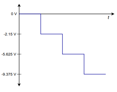
Figure \(\PageIndex{2}\): Output with four digital words.
If this sequence is repeated over and over, the waveform of Figure \(\PageIndex{3}\) is the result. Note that a “stair-step” type wave is created. You might also think of this as a very rough form of a ramp function. A better ramp would be produced if we used all of the available values for the input sequence, as in \(0000, 0001, 0010, 0011, \dots , 1111\). In order to remove the negative DC offset and make the signal bipolar, all we need to do is pass the signal through a coupling capacitor. The frequency of this waveform is controlled by the rate at which the words are fed to the converter. Note that by increasing the resolution and the number of words fed to the converter per cycle, a very close approximation to the ideal ramp function may be achieved. For that matter, by changing the input words to other sequences, we can create a wide variety of output wave shapes. This is the concept behind the digital arbitrary function generator. An arbitrary function generator allows you to create wave shapes beyond the simple sine/square/triangle found on the typical laboratory function generator. We'll take a closer look at this particular piece of test equipment a little later.
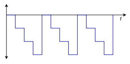
Figure \(\PageIndex{3}\): Cycled output.
In order to increase resolution, it appears that all you need to do to the summing amplifier is add extra channels with larger and larger resistors. Unfortunately, the resistor sizes soon become impractical and another approach is required. For example, a 16-bit system would require that the LSB resistor be equal to 65,536 \(R_f\). One problem is that the resulting small input current may be dwarfed by input bias and offset currents. Also, high component accuracy is needed for the more significant inputs in terms of the input resistors and the drive signals. The excessively large resistors may also contribute added noise. The standard solution to this problem involves of the use of an \(R/2R\) resistive divider network.
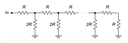
Figure \(\PageIndex{4}\): \(R/2R\) ladder network
An \(R/2R\) network is shown in Figure \(\PageIndex{4}\). This circuit exhibits the unique attribute of constant division by 2 for each stage. You may think of this as either a division of voltage at each successive node or a division of current in each successive leg. An example of a four stage (i.e., four-bit) network is shown in Figure \(\PageIndex{5}\).
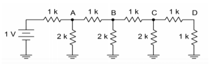
Figure \(\PageIndex{5}\): A 4-stage ladder.
In order to find the voltage at any given node, the loading effects of the following stages must be taken into account. This is much easier to do than it first appears. If we need to find the voltage at point \(A\), we must first find the resistance in parallel with the initial 2 \(k\Omega\) resistor. A quick inspection shows that each stage is loaded by the following stages, so it is easiest if we start at the last stage and work toward the input. The effective resistance to the right of node \(C\) is 1 \(k\Omega\) in series with 1 \(k\Omega\), or 2 \(k\Omega\). This resistance is placed in parallel with the 2 \(k\Omega\) resistor seen from node \(C\) to ground. The result is 1 \(k\Omega\). In other words, from \(C\) to ground, we see 1 \(k\Omega\). This creates a 2:1 voltage divider with the 1 \(k\Omega\) resistor placed from \(B\) to \(C\), so the voltage at \(C\) must be half the voltage at \(B\). This also points up the fact that the current entering node \(C\) splits into two equal portions: one that travels towards point \(D\), and the other that travels through the 2 \(k\Omega\) resistor to ground. This is shown graphically in Figure \(\PageIndex{6}\).
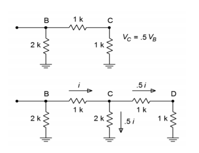
Figure \(\PageIndex{6}\): Ladder analysis. a. Equivalent circuit (top). b. Current division (bottom).
If you look at the equivalent circuit section of Figure \(\PageIndex{6}\), you will notice that this portion now looks exactly like the final portion of the original network. That is, every time a section is simplified and analyzed, the result will be a halving of voltage and current. It is already apparent that the voltage at \(D\) must be half the voltage at \(C\), which in turn, must be half the voltage at \(B\). As you can now prove, it follows that the voltage at \(B\) must be half the voltage at \(A\). In a similar fashion, the current passing through each \(2R\) leg is half the preceding current. (For current division, the final section is not used to derive a current since it will be equal to the value in the preceding stage.) The halving of current is just what is needed for the binary representation of the digital input word.
Adapting the \(R/2R\) network to the DA converter is relatively easy. The network is fed from a stable current source, with each \(2R\) element feeding into a summing amplifier. In series with each \(2R\) element is a solid-state switch, which sets the appropriate logic level. This is shown in Figure \(\PageIndex{7}\), with the network effectively on its side. When a logical high is presented to a given bit, the switch is closed and current flows through the \(2R\) element and into the op amp. Note that the right end of the resistor is effectively at ground, as the summing node of the op amp is a virtual ground. If a logical low is presented, the switch shunts the current to ground, bypassing the op amp. In this way, the appropriately weighted currents are summed and used to produce the output voltage.
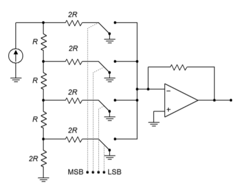
Figure \(\PageIndex{7}\): Converter with R/2R ladder.
This technique offers several advantages over the simpler weighted gain version. First, all branches are fed by one common current source. Because of this, there is no need for output level matching. Second, only two different values of resistors are required for any number of bits used, rather than the impractically wide range seen earlier. It is more economical to control the tolerance of just two different parts than 12 or 16. Note that small input currents are still generated for the least significant bits, so attention to input bias and offset currents remains important.
12.4.1: Practical Digital-to-Analog Converter Limits
Perhaps the most obvious limit associated with the DA converter is its speed. The op amp used in the DAC must be much faster than the final signals it is meant to produce. A given output waveform may contain several dozen individual sample points per cycle. The op amp must respond to each sample point. Consequently, wide bandwidth and high slew rates are required.
Integrated DAC spec sheets offer a few important parameters of which you should be aware. First of all, there is conversion speed. This figure tells how long it takes the DAC to turn the digital input word into a stable analog output voltage. This sets the maximum data rate. Next come the accuracy and resolution. Resolution indicates the number of discrete steps that may be produced at the output, and is set by the number of bits available. This is not the same as accuracy. Accuracy is actually comprised of several different factors including offset error, error, and nonlinearity. Offset error is normally measured by applying the all-zero input word and then measuring the output signal. Ideally, this signal will be zero volts. The deviation from zero is taken as the offset error. This has the effect of making all output levels inaccurate by a constant voltage. Offset error is relatively easy to compensate for in many applications by applying an equal offset of opposite polarity. Gain error is a deviation that affects each output level by a constant percentage. It is as if the signal were passed through a small amplifier or attenuator. This error may be compensated for by using an amplifier with a gain equal to the reciprocal of the error. The two gains will effectively cancel. The effect of offset and gain error are shown in Figures \(\PageIndex{8}\) and \(\PageIndex{9}\).
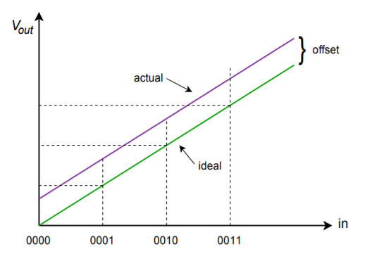
Figure \(\PageIndex{8}\): Offset error only.
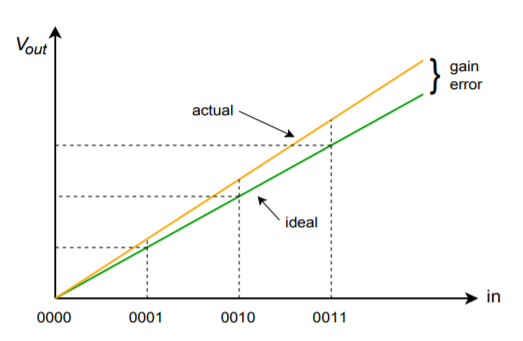
Figure \(\PageIndex{9}\): Gain error only.
Nonlinearity errors may be broken into two forms: integral nonlinearity and differential nonlinearity. Integral nonlinearity details the maximum offset between the ideal outputs and the actual outputs for all possible inputs. Differential nonlinearity details the maximum output deviation relative to one LSB caused by two adjacent input words. If differential nonlinearity is beyond \(\pm 1\) LSB, the system may be non-monotonic. In other words, a higher digital input word may actually produce a lower analog output voltage. These two forms of error are shown in Figure \(\PageIndex{10}\). Note that it is possible to have high integral nonlinearity and yet still have modest differential nonlinearity. This is the case in Figure \(\PageIndex{10b}\).
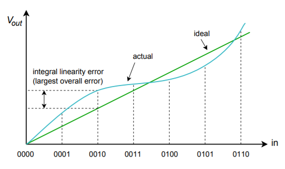
Figure \(\PageIndex{10a}\): Linearity error Integral linearity error.
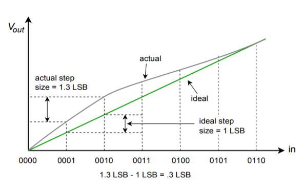
Figure \(\PageIndex{10b}\): Linearity error (continued) Differential linearity error (relative-adjacent error).
As you can see, accuracy is dependent on rather complex factors. In an effort to boil this down to a single number, some manufactures give an effective number of bits specification. For example, a 16-bit DAC may be specified as having 14-bit accuracy. This means that the 14 most significant bits behave in the idealized fashion, but the lowest 2 bits may be swamped out by linearity errors. Another spec that you will sometimes see is no missing codes. This means that for every increase in the input word, there will be an appropriate positive output level change.
In practice, the standard DA converter is used with an output filter. As you can see from the previous figures, the waveforms produced by the DAC contain a stair-step side effect. Generally, this is not desirable. The abrupt changes in output level indicate that higher frequency components are present. All components above the Nyquist rate should be filtered out with an appropriate low-pass filter. This filter is sometimes referred to as a reconstruction or smoothing filter. In an improperly designed system, the reconstruction filter will remove some of the highest in-band frequency components (i.e., components immediately below the Nyquist frequency). To compensate for this, logic levels are often latched to the DAC for shortened periods, thus creating a more spiked appearance, rather than the stair-step form. This effect is shown in Figure \(\PageIndex{11}\). Although this spiked waveform appears to be less desirable than the stair-step form, it creates higher levels for the uppermost components, and after filtering, the result is a smoother overall frequency response.
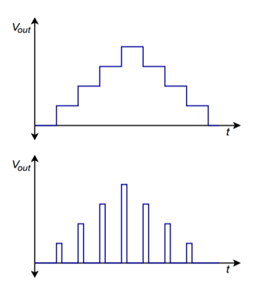
Figure \(\PageIndex{11}\): Output reconstruction. a. Full period latch (top). b. Partial period latch (bottom).
To further increase the quality of the output waveform, a technique known as oversampling is sometimes employed. The basic idea is to create new sample points in between the existing ones. The result is a much denser data rate, which hopefully, will yield more exacting results after filtering. Also, the higher data rate may loosen the requirements of the reconstruction filter. A typical system might use four times oversampling, meaning that the output data rate is four times the original. Therefore, for each input word, three new words have to be added. This effect is shown in Figure \(\PageIndex{12}\).
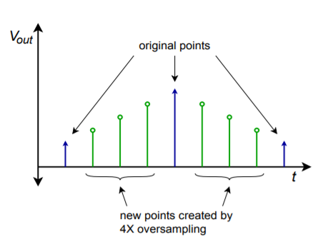
Figure \(\PageIndex{12}\): Oversampled output.
There are a number of ways to create the new sample points. The most obvious way is via simple interpolation, but this does not achieve the best results. Another technique involves initializing the new values to zero and then passing the data stream through a digital low-pass filter, which effectively calculates the proper values. An extension of the oversampling principle is the delta-sigma technique. In delta-sigma, very high rates of oversampling are used in conjunction with specialized digital filter algorithms. The algorithms essentially trade the higher data rate for a slower rate with increased resolution. The design and analysis of delta-sigma systems is fairly advanced and is beyond the scope of this text. Suffice to say that these techniques can increase the quality of the output signal and are widely used in applications such as high-quality audio CD and DVD players.
12.4.2: Digital-to-Analog Converter Integrated Circuits
There are many possible applications for digital-to-analog converters, and a number of different chips have evolved to meet specific needs. Generally, you can group these into specific classes, such as high speed, high resolution, or low cost. We will examine three representative types. The devices we will look at are the DAC0832; a basic 8-bit unit, the DAC7545; a microprocessor-compatible 12-bit unit, and the PCM1716; a 24-bit high-quality converter used in the audio industry.
DAC0832
This IC is a popular microprocessor-compatible 8-bit converter. The DAC0830 and DAC0831 are similar, but with somewhat reduced performance. It is a multiplying DAC. In other words, the output signal is a function of the digital input word and a reference input. In some applications, the reference input is not fixed, but rather, is a variable input signal. A feature list and pin-out are shown in Figure \(\PageIndex{13}\). Notable items are a settling time of only 1 \(\mu\)s, low power requirements, and high linearity. The DAC0832 may be used in either stand-alone mode or with a microprocessor. The switching waveforms are shown in Figure \(\PageIndex{14}\).
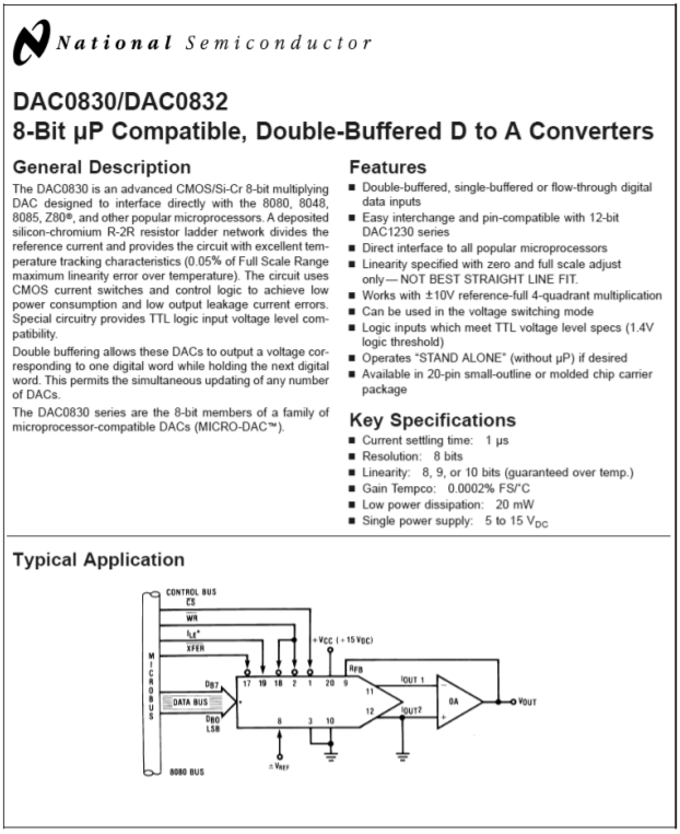
Figure \(\PageIndex{13}\): DAC0832. Reprinted courtesy of Texas Instrutment
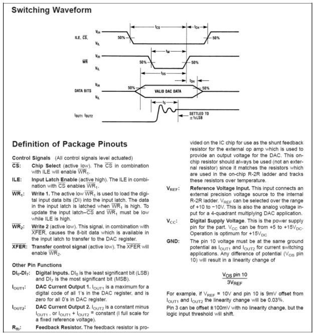
Figure \(\PageIndex{14}\): DAC0832 switching waveforms Reprinted courtesy of Texas Instrutments
An interesting application of the DAC0832 can be found in Figure \(\PageIndex{15}\). Basically, this is a digitally-controlled state variable filter.
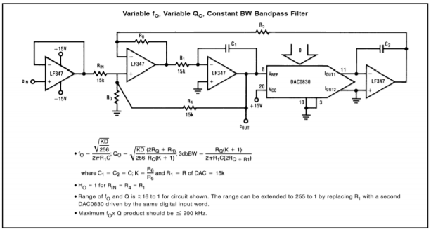
Figure \(\PageIndex{15}\): DAC0832 state variable filter application. Reprinted courtesy of Texas Instrutments
Note that the converter replaces the input resistor of the second integrator. Normally, that resistor would be used to convert the output voltage of the first integrator into an input current for the second integrator. This job is now handled by the DAC0832. The digital input word effectively sets the voltage-to-current conversion. Thus, a change in the input word alters the tuning frequency of the filter just as a potentiometer. Compare this circuit to the OTA-based voltage-controlled filter from Chapter Eleven. Conceptually, they are very similar.
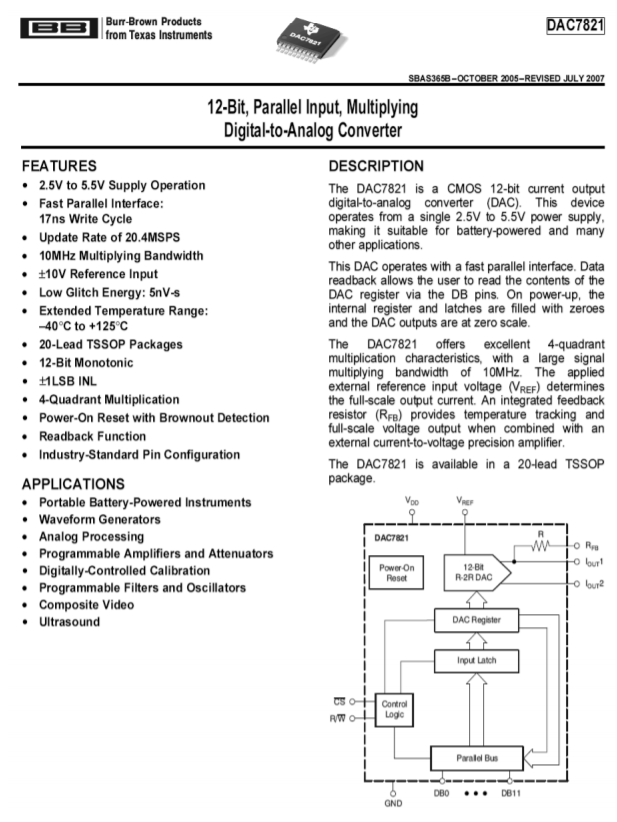
Figure \(\PageIndex{16}\): DAC7821. Reprinted courtesy of Texas Instruments
DAC7821
The DAC7821 is a fairly standard 12-bit linear converter and is shown in Figure \(\PageIndex{16}\). Its interesting aspects are that it is a multiplying converter and that it is microprocessor-compatible. The multiplying effect comes from the fact that a reference is used to drive the \(R/2R\) ladder network. If the reference is changed, the output is effectively rescaled. Consequently, you can think of the output signal as equal to the reference value times the digital input word. You may also think of this as a form of “digital volume control”.
With the inclusion of a few extra logic lines, the IC has become microprocessor compatible. This means that the DAC7821 has chip select and read/write lines along with the 12 data input lines. This allows the converter to be connected directly to the microprocessor data bus. By using memory-mapped I/O, the microprocessor can write data to the converter just as it writes data to memory. A 16-bit microprocessor system can present the converter with all of the data it needs during one write cycle, however an 8-bit microprocessor will need two write cycles and some form of latch. One address may be used for the lower 8 bits, and another address for the remaining 4 bits. A simplified system is shown in Figure \(\PageIndex{17}\) using an 8-bit microprocessor.
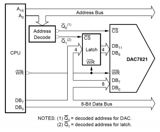
Figure \(\PageIndex{17}\): Microprocessor to DAC7821 interface. Reprinted courtesy of Texas Instruments
PCM5242
The PCM5242 is a stereo 24-bit converter designed specifically for high-quality digital audio applications. It comes in a VQFN (Very thin Quad Flat No-lead) package. A block diagram and feature list are shown in Figure \(\PageIndex{18a}\). Unlike the other converters, the PCM5242 features serial input of data, not parallel. It includes its own on-board serial conversion circuitry and logic. This technique helps to reduce system cost. It is also surprisingly convenient as many specialized digital signal processing ICs that might be used with the PCM5242 utilize a serial-type output. This may be fed directly into the PCM5242 in 16-, 24-, or 32-bit format.
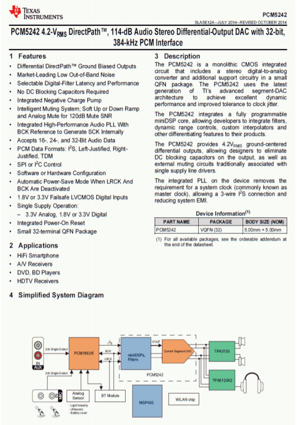
Figure \(\PageIndex{18a}\): PCM5242. Reprinted courtesy of Texas Instruments
The PCM5242 specification sheet is shown in Figure \(\PageIndex{18b}\). Note that this device is specified with sampling rates from 48 kHz to 192 kHz. Total harmonic distortion plus noise is typically 94 dB below a full-scale output when used with any of these sample rates. Due to its high resolution and 114 dB dynamic range, extra care must be taken during circuit layout to avoid hum pickup and RF interference.
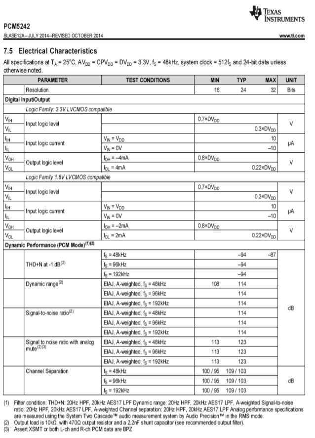
Figure \(\PageIndex{18b}\): PCM5242 specifications. Reprinted courtesy of Texas Instruments
12.4.3: Applications of Digital-to-Analog Converter Integrated Circuits
Example \(\PageIndex{1}\)
Perhaps the first thing many people think of when they hear the terms digital or digitized, is the audio compact disk, or CD for short. Home CD players are excellent examples of the use of precision DA circuitry in our everyday lives. Music data is stored on the CD with 16-bit resolution and a sampling rate of 44.1 kHz. This produces a Nyquist frequency of 22.05 kHz, which is high enough to encompass the hearing range of most humans. Error correction and auxiliary data is also stored on the disk. The data is stored on disk in the form of very tiny pits, which are read by a laser. The signal is then converted into the common electronic logic form where it is checked for error and adjusted as need be. The data stream is then fed to the DA converter for audio reconstruction. A single converter may be multiplexed between the two stereo channels, or two dedicated converters may be used. Oversampling in the range of 2X to 8X is often used for improved signal quality. A block diagram of the system is shown in Figure \(\PageIndex{19}\). The actual DAC portion seems almost trivial when compared to some of the more sophisticated elements.
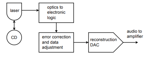
Figure \(\PageIndex{19}\): Audio compact disk playback system.
The storage density of the optical CD is quite remarkable. This small disk (less than 5 inches in diameter) can hold 70 minutes of music. Ignoring the auxiliary data, we can quickly calculate the total storage. We have two channels of 16-bit data, or 32 bits (4 bytes) per sample point. There are 44,100 samples per second for 70 minutes, yielding 185.22 megasamples. The total data storage is 5.927 gigabits, or 741 megabytes.
Example \(\PageIndex{2}\)
As we have already mentioned, it is possible to connect DACs directly to microprocessor systems. Furthermore, the microprocessor may write to the DAC with no more effort than writing to a memory location. The microprocessor can write any series of data words we desire out to the DAC and can repeat a sequence virtually forever. Given this ability, we can make an arbitrary waveform generator. Instead of being locked into a set of predefined wave shapes as on ordinary function generators, this system allows for all manner of wave shapes. The accuracy and flexibility of the system will depend on its speed and the available DAC resolution.
The basic idea is one of table look-up. For example, let's say that we have a 16-bit system. We will create a table of data values for one cycle of the output waveform. For convenience sake, we might make the table size a handy power of 2, such as 256. In other words, a single output cycle will be chopped into 256 discrete time chunks. It is obvious, then, that the converter must be a few hundred times faster than the highest fundamental that we wish to produce. By increasing or decreasing the output data rate, we can change the frequency of the output fundamental. This is known as a variable sample rate technique. It is also possible to change the fundamental frequency with a fixed rate technique (this is somewhat more complex, but does offer certain advantages). An output flow chart is shown in Figure \(\PageIndex{20}\).
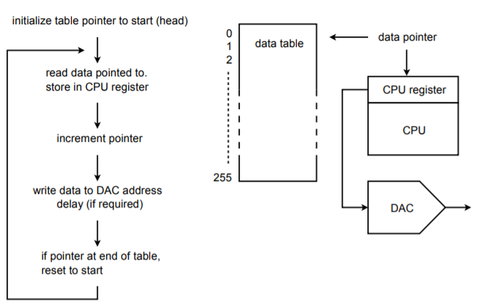
Figure \(\PageIndex{20}\): Arbitrary waveform generator.
Upon initialization, an address pointer is set to the starting address of the data table. The CPU reads the data from the table via the pointer. The pointer is incremented so that it now points to the next element in the table. (Some CPUs offer a post-increment addressing mode so that both steps may be performed in a single instruction.) Next, the CPU writes the data to the special DAC address. At this point, some form of software/hardware delay is invoked that sets the output data rate. After the delay, the CPU reads the next data element via the pointer and continues as in the first run. Once the 256th element is sent out, the pointer is reset to the start of the table and the process continues on. In this way, the table can be thought of as circular, or never-ending. If the system software is written in a higher level language, the pointer/data table may be implemented as a simple array where the array index is set by a counter. This will not be as efficient as a direct assembly level approach, though.
The real beauty of this system is that the data table may contain virtually any sequence of data. The data could represent a sine, pulse, triangle, or other standard function. More importantly, the data could represent a sine wave with an embedded noise transient, or a signal containing a hum component just as easily. This data could come from three basic sources. First, the data table can be filled through direct computation if the time-domain equation of the desired function is known. Second, the data could be manufactured by the user through some form of interaction with a computer, perhaps with a mouse or drawing pad. Finally, the data may be derived from a real-world signal. That is, an analog-to-digital converter may be used to record the signal in digital form. The data may then be loaded into the table and played back repeatedly. The arbitrary waveform generator allows its user to test circuits and systems with a range of wave shapes that would be impossible or impractical to generate otherwise.
Example \(\PageIndex{3}\)
Under computer control, DA converters can be used as part of an automated test equipment system. In order to fully characterize an electronic product, a number of individual tests need to be run. Setting up each individual test can be somewhat time consuming and is subject to operator error. Automating this procedure may improve repeatability and decrease testing time. There are many ways in which this process may be automated. We'll look at one approach.
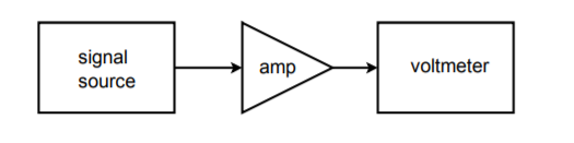
Figure \(\PageIndex{21}\): Simple test setup.
Let's assume that we would like to make frequency response measurements for an amplifier at 20 different frequencies. A circuit test system appropriate for this job is shown in Figure \(\PageIndex{21}\). To perform this test manually requires 20 distinct settings of the source signal, and 20 corresponding output readings. This can prove to be rather tedious if many units are to be tested. It would be very handy if there was some way in which the source frequency could be automatically changed to preset values. This is not particularly difficult. Most modern sources have control voltage inputs that may be used to set the frequency. The required control voltage can be created and accurately set through the use of a computer and DA converter. The computer can be programmed to send specific digital words to the DAC, which in turn feeds the signal source control input. In other words, the data word directly sets the frequency of the signal source. The computer can be programmed to send virtually any sequence of data words at almost any rate and do it all without operator intervention. All the operator needs to do is start the process. Test repeatability is very high with a system like this. A block diagram of this system is shown in Figure \(\PageIndex{22}\).
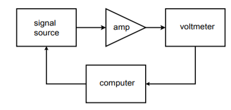
Figure \(\PageIndex{22}\): Automated test setup.
In order to record the data, the voltmeter may be connected to a strip chart recorder, or better yet, back to the computer. The data may be sent to the computer in digital form if the voltmeter is of fairly advanced design, or, with the inclusion of an analog-to-digital converter, the output signal may be directly sampled and manipulated by the computer. In either case, data files may be created for each unit tested and stored for later use. Also, convenient statistical analysis may be performed quickly at the end of a test batch. Note that because the DA converter only generates a control signal, very high resolution and low distortion is normally not required. If a high resolution converter is used, it is possible to create the test signals in the computer (as in the arbitrary function generator), and dispense with the signal source.
The automated test system is only one possible application of instrument control. Another interesting example is in the generation of laser “light shows”. A block diagram of a simplified system is shown in Figure \(\PageIndex{23}\). In order to create the complex patterns seen by the audience, a laser beam is bounced off of tiny moving mirrors. The mirrors may be mounted on something as simple as a galvanometer. The galvanometer is fed by a DAC. The pattern that the laser beam makes is dependent on how the galvanometer moves the mirror, which is in turn controlled by the data words fed to the DAC. In practice, several mirrors may be used to deflect the beam along three axes.
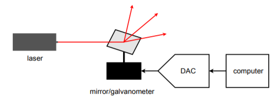
Figure \(\PageIndex{23}\): Computer-controlled lighting.
DA converters can be used to adjust any device with a control-voltage type input. Also, they may be used to control electromechanical devices that respond to an applied voltage. Their real advantage is the repeatability and flexibility they offer.