Engineering LibreTexts

11.2: Simplified AC Model of the JFET

  • Page ID
    25320
  • \( \newcommand{\vecs}[1]{\overset { \scriptstyle \rightharpoonup} {\mathbf{#1}} } \) \( \newcommand{\vecd}[1]{\overset{-\!-\!\rightharpoonup}{\vphantom{a}\smash {#1}}} \)\(\newcommand{\id}{\mathrm{id}}\) \( \newcommand{\Span}{\mathrm{span}}\) \( \newcommand{\kernel}{\mathrm{null}\,}\) \( \newcommand{\range}{\mathrm{range}\,}\) \( \newcommand{\RealPart}{\mathrm{Re}}\) \( \newcommand{\ImaginaryPart}{\mathrm{Im}}\) \( \newcommand{\Argument}{\mathrm{Arg}}\) \( \newcommand{\norm}[1]{\| #1 \|}\) \( \newcommand{\inner}[2]{\langle #1, #2 \rangle}\) \( \newcommand{\Span}{\mathrm{span}}\) \(\newcommand{\id}{\mathrm{id}}\) \( \newcommand{\Span}{\mathrm{span}}\) \( \newcommand{\kernel}{\mathrm{null}\,}\) \( \newcommand{\range}{\mathrm{range}\,}\) \( \newcommand{\RealPart}{\mathrm{Re}}\) \( \newcommand{\ImaginaryPart}{\mathrm{Im}}\) \( \newcommand{\Argument}{\mathrm{Arg}}\) \( \newcommand{\norm}[1]{\| #1 \|}\) \( \newcommand{\inner}[2]{\langle #1, #2 \rangle}\) \( \newcommand{\Span}{\mathrm{span}}\)\(\newcommand{\AA}{\unicode[.8,0]{x212B}}\)

    An AC model of the JFET is shown in Figure \(\PageIndex{1}\). This is essentially the same model as was used for DC analysis. Once again, we have a voltage-controlled current source situated in the drain. The reverse-biased junction shows up as a very large resistance, \(r_{GS}\).

    clipboard_edd135f59ee5c119981e61f8d048e0826.png

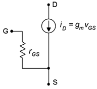
    Figure \(\PageIndex{1}\): AC model of JFET.

    It is worth mentioning that this model is suitable only for low frequencies. At higher frequencies, device capacitances can play a major role in the response of the amplifier. There are three device capacitances not shown in the Figure that shunt each pair of terminals: \(C_{GS}\), \(C_{DG}\) and \(C_{DS}\). On a data sheet, the “lumped” capacitances are often given. These are \(C_{iss}\), the capacitance looking into the gate with the source and drain shorted to ground: \(C_{iss} = C_{GS} + C_{DG}\); and \(C_{rss}\), the capacitance seen from the drain with the gate and source shorted to ground: \(C_{rss} = C_{DS} + C_{DG}\). As we shall see, these capacitances can have a sizable impact on amplifier characteristics such as \(Z_{in}\).

    The value of transconductance, \(g_m\), will prove to be of particular interest. It is roughly of equal importance to \(r'_e\) in a BJT.1

    References

    1In fact, we can say that \(1/r'_e\) is \(g_m\) for a BJT.


    This page titled 11.2: Simplified AC Model of the JFET is shared under a CC BY-NC-SA 4.0 license and was authored, remixed, and/or curated by James M. Fiore via source content that was edited to the style and standards of the LibreTexts platform; a detailed edit history is available upon request.