
11.3: Common Source Amplifier
- Page ID
- 25321

The common source amplifier is analogous to the common emitter amplifier. The prototype amplifier circuit with device model is shown in Figure \(\PageIndex{1}\).
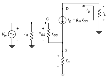
Figure \(\PageIndex{1}\): Common source amplifier with model.
This circuit includes a swamping resistor, \(r_S\). The input signal is presented to the gate terminal while the output is taken from the drain.
11.3.1: Voltage Gain
An equation for the voltage gain, \(A_v\), is developed as follows. First, we start with the fundamental definition, namely that voltage gain is the ratio of \(v_{out}\) to \(v_{in}\), and proceed by expressing these voltages in terms of their Ohm's law equivalents.
\[A_v = \frac{v_{out}}{v_{i n}} = \frac{v_D}{v_G} \\ A_v = \frac{−i_D r_L}{i_D r_S+v_{GS}} \\ A_v = \frac{−g_m v_{GS} r_L}{g_m v_{GS} r_S+v_{GS}} \\ A_v =− \frac{g_m r_L}{g_m r_S+1} \label{11.1} \]
If there is no swamping resistor, the first portion of the denominator drops out and the gain simplifies to \(−g_m \cdot r_L\). The swamping resistor in the source, \(r_S\), plays the same role here as it did in the BJT: it helps to stabilize the gain and reduce distortion. It does so at the expense of voltage gain.
11.3.2: Input Impedance
Referring back to Figure \(\PageIndex{1}\), the input impedance of the amplifier will be \(r_G\) in parallel with the impedance looking into the gate terminal, \(Z_{in(gate)}\). For the non-swamped case, this will be \(r_{GS}\). At low frequencies \(r_{GS}\) is very large, well into the megohms. In most practical circuits, \(r_G\) will be much lower, hence
\[Z_{in} = r_G || r_{GS} \approx r_G \label{11.2} \]
Theoretically, for swamped amplifiers \(Z_{in(gate)}\) will be higher than \(r_{GS}\) but this is a moot point. In either case, it is relatively easy to obtain a high input impedance, certainly much easier than it is for typical single-device BJT amplifiers.
It might be easy to become complacent and simply assume that \(r_G\) sets the input impedance and that's the end of it. This would be a mistake. As mentioned earlier, with impedances this high, we cannot ignore items such as junction capacitance. For example, for a general purpose device a typical value for \(C_{iss}\), the total input capacitance, may be in the vicinity of 5 to 10 pF. This capacitance appears in parallel with \(r_G\). If this amplifier is used for ultrasonic signals, the capacitive reactance, \(X_C\), would be as low as 160 k\(\Omega\) at 100 kHz. Although this is high compared to typical BJT circuits, it's less than the \(R_G\) values commonly used for biasing. At higher frequencies, the situation is even worse as \(X_C\) decreases with frequency. Also, we are ignoring the Miller effect here which makes the situation even worse than even worse, so perhaps we can say that it's even worser, which is a claim we could also make regarding the grammar of this sentence.
11.3.3: Output Impedance
To investigate the output impedance, we'll refer to Figure \(\PageIndex{2}\). This circuit is very similar to that of Figure \(\PageIndex{1}\). The major difference is that the AC load equivalent has been split into its two components, the load itself, \(R_L\), and the drain biasing resistor, \(R_D\).
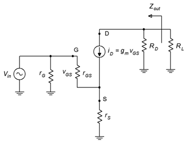
Figure \(\PageIndex{2}\): Output impedance of common source amplifier.
From the vantage point of \(R_L\), peering back into the amplifier we see \(R_D\) in parallel with the impedance at the drain. At the drain we find the current source, \(i_D\). The internal impedance of this equivalent current source is very high compared to typical values for \(R_D\) (hundreds of k\(\Omega\)), therefore we can approximate the output impedance as
\[Z_{out} \approx R_D \label{11.3} \]
It should be noted that all forms of DC bias discussed in the previous chapter are game here. There are a few limitations to be aware of, though. For example, when using constant voltage bias, swamping is not possible as that bias form does not use a source resistor. In contrast, self bias and combination bias include a source resistor so swamping is a possibility, however, \(R_S\) may need to be split and partially bypassed to achieve the desired results. Finally, constant current bias is not well-positioned to use swamping as that would require some additional work to fit in a new \(R_S\) along with the current source. More typically, the current source will just be bypassed with a capacitor to produce a non-swamped amplifier.
Example \(\PageIndex{1}\)
Determine the voltage gain and input impedance for the circuit shown in Figure \(\PageIndex{3}\). Assume \(I_{DSS} = 15\) mA and \(V_{GS(off)} = −3\) V.
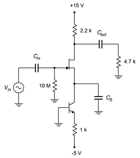
Figure \(\PageIndex{3}\): Circuit for Example \(\PageIndex{1}\).
This is an unswamped common source amplifier with constant current bias. We can determine \(Z_{in}\) via inspection.
\[Z_{i n} = Z_{i n(gate)} || R_G \nonumber \]
\[Z_{i n} \approx 10 M \Omega \nonumber \]
To find the voltage gain, we'll first need to find \(I_D\) and \(g_{m0}\) in order to find \(g_m\).
\[I_D = \frac{∣V_{EE}∣−0.7 V}{R_E} \nonumber \]
\[I_D = \frac{5 V−0.7 V}{1k \Omega} \nonumber \]
\[I_D = 4.3 mA \nonumber \]
\[g_{m0} =− \frac{2 I_{DSS}}{V_{GS (off )}} \nonumber \]
\[g_{m0} =− \frac{30 mA}{−3V} \nonumber \]
\[g_{m0} = 10mS \nonumber \]
Knowing the current and maximum transconductance, we can find \(g_m\) through the use of Equation 10.2.4.
\[\frac{g_m}{g_{m0}} = \sqrt{\frac{I_D}{I_{DSS}}} \nonumber \]
\[g_m = g_{m0} \sqrt{\frac{I_D}{I_{DSS}}} \nonumber \]
\[g_m = 10 mS \sqrt{\frac{4.3mA}{15 mA}} \nonumber \]
\[g_m = 5.35mS \nonumber \]
\[A_v =− \frac{g_m r_L}{g_m r_S+1} \nonumber \]
\[A_v =− \frac{5.35 mS(2.2k \Omega || 4.7 k\Omega)}{5.35mS \times 0 \Omega +1} \nonumber \]
\[A_v =−8.02 \nonumber \]
Example \(\PageIndex{2}\)
Determine the voltage gain and input impedance for the circuit shown in Figure \(\PageIndex{3}\). Assume \(I_{DSS} = 24\) mA and \(V_{GS(off)} = −4\) V.
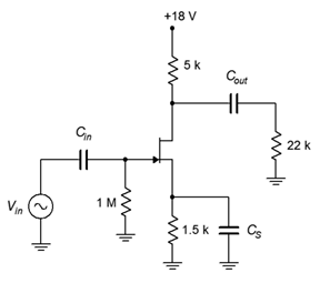
Figure \(\PageIndex{4}\): Circuit for Example \(\PageIndex{2}\)
This is an unswamped common source amplifier with self bias. Once again, we can determine \(Z_{in}\) via inspection.
\[Z_{i n} = Z_{i n(gate)} || R_G \nonumber \]
\[Z_{i n} \approx 1 M\Omega \nonumber \]
To find the voltage gain, we'll first need to find \(g_{m0}\). Also, we can take a shortcut and find the normalized drain current from the self bias graph instead of finding \(I_D\) itself.
\[g_{m0} =− \frac{2 I_{DSS}}{V_{GS (off )}} \nonumber \]
\[g_{m0} =− \frac{48 mA}{−4 V} \nonumber \]
\[g_{m0} = 12mS \nonumber \]
\(R_S\) is 1.5 k\(\Omega\), therefore \(g_{m0}R_S = 18\). From the self bias graph this produces a normalized drain current of 0.08.
\[g_m = g_{m0} \sqrt{\frac{I_D}{I_{DSS}}} \nonumber \]
\[g_m = 12mS\sqrt{0.08} \nonumber \]
\[g_m = 3.4 mS \nonumber \]
Again, there is no swamping so \(r_S = 0\). The gain formula reduces to
\[A_v =−g_m r_L \nonumber \]
\[A_v =−3.4mS(22k \Omega || 5k \Omega) \nonumber \]
\[A_v =−13.9 \nonumber \]
We will now turn our attention to the effect of swamping. As in the BJT case, we expect to sacrifice gain and in return, see an improvement in distortion. We shall examine this through the use of a simulation.
Computer Simulation
A common source amplifier using self bias is entered into the simulator as shown in Figure \(\PageIndex{5}\).
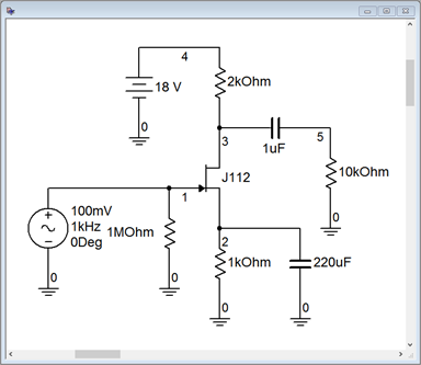
Figure \(\PageIndex{5}\): Common source amplifier in simulator.
Reasonable device values for this model are \(I_{DSS} = 40\) mA and \(V_{GS(off)} = −2.3\) V. Based on these we find
\[g_{m0} =− \frac{2 I_{DSS}}{V_{GS(off )}} \nonumber \]
\[g_{m0} =− \frac{80 mA}{−2.3V} \nonumber \]
\[g_{m0} = 34.8mS \nonumber \]
Given \(R_S = 1\) k\(\Omega\), the self-bias equation yields
\[I_D = 2 I_{DSS} \left( \frac{1+g_{m0} R_S − \sqrt{1+2 g_{m0} R_S}}{( g_{m0} R_S )^2} \right) \nonumber \]
\[I_D = 2 I_{DSS} \left( \frac{1+34.8 −\sqrt{1+2 \times 34.8}}{(34.8)^2} \right) \nonumber \]
\[I_D = 1.81mA \nonumber \]
\[g_m = g_{m0} \sqrt{\frac{I_D}{I_{DSS}}} \nonumber \]
\[g_m = 34.8mS \sqrt{\frac{1.81 mA}{40 mA}} \nonumber \]
\[g_m = 7.4 mS \nonumber \]
\[A_v =−g_m r_L \nonumber \]
\[A_v =−7.4mS(2k \Omega || 10k \Omega) \nonumber \]
\[A_v =−12.3 \nonumber \]
The results of a transient analysis are shown in Figure \(\PageIndex{6}\) for a 100 mV peak input signal.
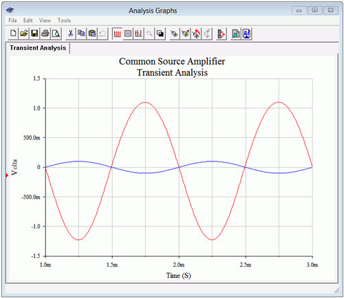
Figure \(\PageIndex{6}\): Transient analysis of the common source amplifier.
First, the inversion between the input (blue trace) and output (red trace) is obvious. Also, some distortion is evident in the output waveform. Inspecting the positive and negative peaks shows that the positive peaks are are a little more broad than the negative ones and don't quite reach the same magnitude. The averaged gain is about −11.75, around 5% low from the estimate and not too bad considering the distortion.
The simulation is run a second time, but this time around the 1 k\(\Omega\) source resistor is split into a 200 \(\Omega\)/800 \(\Omega\) pair with only the 800 \(\Omega\) being bypassed. The DC bias does not change leaving \(g_m\) untouched, but the new 200 \(\Omega\) swamping resistor drops the gain to
\[A_v =− \frac{g_m r_L}{g_m r_S+1} \nonumber \]
\[A_v =− \frac{7.4 mS(2 k \Omega || 10 k \Omega)}{7.4mS \times 200 \Omega +1} \nonumber \]
\[A_v =−4.96 \nonumber \]
The output signal from the simulator is shown in Figure \(\PageIndex{6}\).
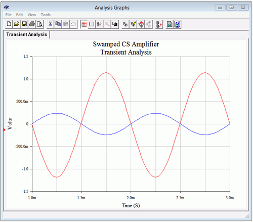
Figure \(\PageIndex{7}\): Transient analysis of the swamped common source amplifier.
The input signal was raised to 240 mV peak in order to keep the output signals of the two versions at the same amplitude. The symmetry appears to be better here and the gain works out to −4.85, just a few percent low.
Total harmonic distortion (THD) analysis is performed next. The results are shown in Figures \(\PageIndex{8}\) and \(\PageIndex{9}\). To keep the comparison fair, the input levels are adjusted to maintain similar output voltages. The non-swamped results are seen in Figure \(\PageIndex{8}\), and as expected based on the waveform asymmetry, the THD is relatively high at roughly 4%. The swamped version scores better at just over 1.6%, although this is still not stellar performance.
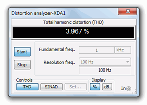
Figure \(\PageIndex{8}\): THD of common source amplifier.
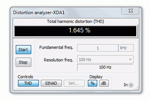
Figure \(\PageIndex{9}\): THD of swamped common source amplifier.
It is interesting to note that while the voltage gain of the swamped amplifier has dropped to 41% of the non-swamped gain, the THD has dropped to 41% of the nonswamped THD. In fact, given the square-law nature of the characteristic curve, we would expect the distortion to be lower if we used smaller signals. To verify this, the THD simulation is run again for the swamped amplifier, but now using an input signal ten times smaller at only 24 mV peak. The result is shown in Figure \(\PageIndex{10}\).
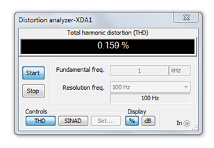
Figure \(\PageIndex{10}\): THD of swamped common source amplifier with reduced signal level.
The resulting THD is markedly lower for an order of magnitude improvement. We're now at least approaching “hi-fi” territory.