
11.4: Common Drain Amplifier
- Page ID
- 25322

The common drain amplifier is analogous to the common collector emitter follower. The JFET version is also known as a source follower. The prototype amplifier circuit with device model is shown in Figure \(\PageIndex{1}\). As with all voltage followers, we expect a non-inverting voltage gain close to unity, a high \(Z_{in}\) and low \(Z_{out}\).
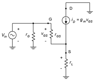
Figure \(\PageIndex{1}\): Common drain (source follower) prototype.
The input signal is presented to the gate terminal while the output is taken from the source. Many bias circuits may be used here as long as they do not have a grounded source terminal such as constant voltage bias.
11.4.1: Voltage Gain
In order to develop an equation for the voltage gain, \(A_v\), we follow the same path we took with the common source amplifier earlier in this chapter. First, we start with the fundamental definition, namely that voltage gain is the ratio of \(v_{out}\) to \(v_{in}\), and proceed by expressing these voltages in terms of their Ohm's law equivalents.
\[A_v = \frac{v_{out}}{v_{i n}} = \frac{v_S}{v_G} \\ A_v = \frac{i_D r_L}{i_D r_L+v_{GS}} \\ A_v = \frac{g_m v_{GS} r_L}{g_m v_{GS} r_L+v_{GS}} \\ A_v = \frac{g_m r_L}{g_m r_L+1} \label{11.4} \]
Equation \ref{11.4} is very similar to the gain equation derived for the swamped common source amplifier; the notable changes being the lack of the minus sign indicating that this circuit does not invert the signal, and \(r_L\) replacing \(r_S\) in the denominator. It is worth remembering that \(r_L\) here is the AC source resistance while in the common source amplifier \(r_L\) is the AC drain resistance. To avoid potential confusion, this equation could also be written as
\[A_v = \frac{g_m r_S}{g_m r_S+1} \label{11.4b} \]
In any event, the goal is to make sure that \(g_mr_S \gg 1\). By doing so, the voltage gain will be very close to unity.
11.4.2: Input Impedance
The analysis for common drain input impedance is virtually identical to that for the swamped common source amplifier. The result is replicated here for convenience.
\[Z_{in} = r_G || r_{GS} \approx r_G \label{11.5} \]
11.4.3: Output Impedance
In order to investigate the output impedance, we'll separate the load resistance from the source bias resistor, as shown in Figure \(\PageIndex{2}\).
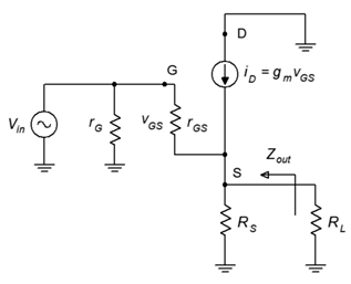
Figure \(\PageIndex{2}\): Common drain output impedance analysis.
From the position of \(R_L\), looking back toward the source we find \(R_S\) in parallel with the impedance looking back into the source terminal. The voltage at this node is \(v_{GS}\) and the current entering this node is \(i_D\). The ratio of the two must yield the impedance looking into the source.
\[Z_{source} = \frac{v_{GS}}{i_D} \\ Z_{source} = \frac{v_{GS}}{g_m v_{GS}} \\ Z_{source} = \frac{1}{g_m} \label{11.6} \]
Therefore, the output impedance is
\[Z_{out} = R_S || \frac{1}{g_m} \label{11.7} \]
We can expect this value to be much smaller than the output impedance of typical common source amplifiers.
Example \(\PageIndex{1}\)
For the follower shown in Figure \(\PageIndex{3}\), determine the input impedance and output voltage. Assume \(V_{in} = 100\) mV, \(I_{DSS} = 30\) mA, \(V_{GS(off)} = −2\) V.
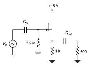
Figure \(\PageIndex{3}\): Circuit for Example \(\PageIndex{1}\).
This is a follower using self bias. We'll find \(g_m\) via the self bias graph.
\[g_{m0} =− \frac{2 I_{DSS}}{V_{GS (off )}} \nonumber \]
\[g_{m0} =− \frac{60 mA}{−2 V} \nonumber \]
\[g_{m0} = 30 mS \nonumber \]
\(R_S\) is 1 k\(\Omega\), yielding 30 for \(g_{m0} R_S\). The normalized drain current from the self bias graph is approximately 0.05.
\[g_m = g_{m0} \sqrt{\frac{I_D}{I_{DSS}}} \nonumber \]
\[g_m = 30mS\sqrt{0.05} \nonumber \]
\[g_m = 6.71 mS \nonumber \]
\[A_v = \frac{g_m r_S}{g_m r_S+1} \nonumber \]
\[A_v = \frac{6.71mS(1 k\Omega || 600 \Omega)}{6.71 mS(1k \Omega || 600\Omega)+1} \nonumber \]
\[A_v = 0.716 \nonumber \]
Thus \(V_{out}\) is 71.6 mV. By inspection, \(Z_{in}\) may be approximated as 2.2 M\(\Omega\).
Example \(\PageIndex{2}\)
For the circuit shown in Figure \(\PageIndex{4}\), determine the input impedance and output voltage. Assume \(V_{in} = 100\) mV, \(I_{DSS} = 36\) mA, \(V_{GS(off)} = 3\) V.
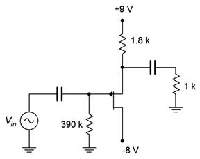
Figure \(\PageIndex{4}\): Circuit for Example \(\PageIndex{2}\).
This follower uses combination bias with a P-channel JFET. Note that the source is at the top. We'll find \(g_m\) via the combination bias graph for \(k = 3\) (\(k = V_{SS} / V_{GS(off)})\).
\[g_{m0} = \frac{2 I_{DSS}}{V_{GS( off )}} \nonumber \]
\[g_{m0} = \frac{72 mA}{3V} \nonumber \]
\[g_{m0} = 24 mS \nonumber \]
\(R_S\) is 1.8 k\(\Omega\), yielding 43.2 for \(g_{m0} R_S\). The normalized drain current from the \(k = 3\) combination bias graph is approximately 0.17.
\[g_m = g_{m0} \sqrt{\frac{I_D}{I_{DSS}}} \nonumber \]
\[g_m = 24 mS \sqrt{0.17} \nonumber \]
\[g_m = 9.9mS \nonumber \]
\[A_v = \frac{g_m r_S}{g_m r_S+1} \nonumber \]
\[A_v = \frac{9.9mS(1 k\Omega || 1.8k \Omega)}{9.9 mS(1k\Omega || 1.8 k\Omega)+1} \nonumber \]
\[A_v = 0.864 \nonumber \]
Thus \(V_{out}\) is 86.4 mV. By inspection, \(Z_{in}\) may be approximated as 390 k\(\Omega\).