
1.2: The Circuit Bit
- Page ID
- 50151

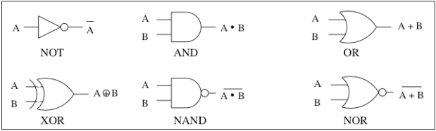
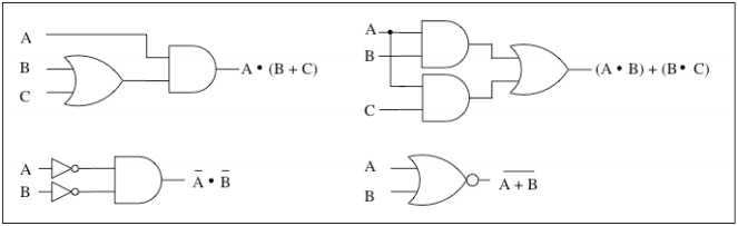
Combinational logic circuits are a way to represent Boolean expressions graphically. Each Boolean function (\(NOT\), \(AND\), \(XOR\), etc.) corresponds to a “combinational gate” with one or two inputs and one output, as shown in Figure 1.1. The different types of gates have different shapes. Lines are used to connect the output of one gate to one or more gate inputs, as illustrated in the circuits of Figure 1.2.
Logic circuits are widely used to model digital electronic circuits, where the gates represent parts of an integrated circuit and the lines represent the signal wiring.
The circuit bit can be copied (by connecting the output of a gate to two or more gate inputs) and
discarded (by leaving an output unconnected).
Combinational circuits have the property that the output from a gate is never fed back to the input of any gate whose output eventually feeds the input of the first gate. In other words, there are no loops in the circuit. Circuits with loops are known as sequential logic, and Boolean algebra is not sufficient to describe them. For example, consider the simplest circuit in Figure 1.3. The inverter (\(NOT\) gate) has its output connected to its input. Analysis by Boolean algebra leads to a contradiction. If the input is 1 then the output is 0 and therefore the input is 0. There is no possible state according to the rules of Boolean algebra. On the other hand, consider the circuit in Figure 1.3 with two inverters. This circuit has two possible states. The bottom circuit has two stable states if it has an even number of gates, and no stable state if it has an odd number.
A model more complicated than Boolean algebra is needed to describe the behavior of sequential logic circuits. For example, the gates or the connecting lines (or both) could be modeled with time delays. The circuit at the bottom of Figure 1.3 (for example with 13 or 15 gates) is commonly known as a ring oscillator, and is used in semiconductor process development to test the speed of circuits made using a new process.