
24.4: Flux Divergence
- Page ID
- 32718
")
\( \newcommand{\vecs}[1]{\overset { \scriptstyle \rightharpoonup} {\mathbf{#1}} } \)
\( \newcommand{\vecd}[1]{\overset{-\!-\!\rightharpoonup}{\vphantom{a}\smash {#1}}} \)
\( \newcommand{\dsum}{\displaystyle\sum\limits} \)
\( \newcommand{\dint}{\displaystyle\int\limits} \)
\( \newcommand{\dlim}{\displaystyle\lim\limits} \)
\( \newcommand{\id}{\mathrm{id}}\) \( \newcommand{\Span}{\mathrm{span}}\)
( \newcommand{\kernel}{\mathrm{null}\,}\) \( \newcommand{\range}{\mathrm{range}\,}\)
\( \newcommand{\RealPart}{\mathrm{Re}}\) \( \newcommand{\ImaginaryPart}{\mathrm{Im}}\)
\( \newcommand{\Argument}{\mathrm{Arg}}\) \( \newcommand{\norm}[1]{\| #1 \|}\)
\( \newcommand{\inner}[2]{\langle #1, #2 \rangle}\)
\( \newcommand{\Span}{\mathrm{span}}\)
\( \newcommand{\id}{\mathrm{id}}\)
\( \newcommand{\Span}{\mathrm{span}}\)
\( \newcommand{\kernel}{\mathrm{null}\,}\)
\( \newcommand{\range}{\mathrm{range}\,}\)
\( \newcommand{\RealPart}{\mathrm{Re}}\)
\( \newcommand{\ImaginaryPart}{\mathrm{Im}}\)
\( \newcommand{\Argument}{\mathrm{Arg}}\)
\( \newcommand{\norm}[1]{\| #1 \|}\)
\( \newcommand{\inner}[2]{\langle #1, #2 \rangle}\)
\( \newcommand{\Span}{\mathrm{span}}\) \( \newcommand{\AA}{\unicode[.8,0]{x212B}}\)
\( \newcommand{\vectorA}[1]{\vec{#1}} % arrow\)
\( \newcommand{\vectorAt}[1]{\vec{\text{#1}}} % arrow\)
\( \newcommand{\vectorB}[1]{\overset { \scriptstyle \rightharpoonup} {\mathbf{#1}} } \)
\( \newcommand{\vectorC}[1]{\textbf{#1}} \)
\( \newcommand{\vectorD}[1]{\overrightarrow{#1}} \)
\( \newcommand{\vectorDt}[1]{\overrightarrow{\text{#1}}} \)
\( \newcommand{\vectE}[1]{\overset{-\!-\!\rightharpoonup}{\vphantom{a}\smash{\mathbf {#1}}}} \)
\( \newcommand{\vecs}[1]{\overset { \scriptstyle \rightharpoonup} {\mathbf{#1}} } \)
\(\newcommand{\longvect}{\overrightarrow}\)
\( \newcommand{\vecd}[1]{\overset{-\!-\!\rightharpoonup}{\vphantom{a}\smash {#1}}} \)
\(\newcommand{\avec}{\mathbf a}\) \(\newcommand{\bvec}{\mathbf b}\) \(\newcommand{\cvec}{\mathbf c}\) \(\newcommand{\dvec}{\mathbf d}\) \(\newcommand{\dtil}{\widetilde{\mathbf d}}\) \(\newcommand{\evec}{\mathbf e}\) \(\newcommand{\fvec}{\mathbf f}\) \(\newcommand{\nvec}{\mathbf n}\) \(\newcommand{\pvec}{\mathbf p}\) \(\newcommand{\qvec}{\mathbf q}\) \(\newcommand{\svec}{\mathbf s}\) \(\newcommand{\tvec}{\mathbf t}\) \(\newcommand{\uvec}{\mathbf u}\) \(\newcommand{\vvec}{\mathbf v}\) \(\newcommand{\wvec}{\mathbf w}\) \(\newcommand{\xvec}{\mathbf x}\) \(\newcommand{\yvec}{\mathbf y}\) \(\newcommand{\zvec}{\mathbf z}\) \(\newcommand{\rvec}{\mathbf r}\) \(\newcommand{\mvec}{\mathbf m}\) \(\newcommand{\zerovec}{\mathbf 0}\) \(\newcommand{\onevec}{\mathbf 1}\) \(\newcommand{\real}{\mathbb R}\) \(\newcommand{\twovec}[2]{\left[\begin{array}{r}#1 \\ #2 \end{array}\right]}\) \(\newcommand{\ctwovec}[2]{\left[\begin{array}{c}#1 \\ #2 \end{array}\right]}\) \(\newcommand{\threevec}[3]{\left[\begin{array}{r}#1 \\ #2 \\ #3 \end{array}\right]}\) \(\newcommand{\cthreevec}[3]{\left[\begin{array}{c}#1 \\ #2 \\ #3 \end{array}\right]}\) \(\newcommand{\fourvec}[4]{\left[\begin{array}{r}#1 \\ #2 \\ #3 \\ #4 \end{array}\right]}\) \(\newcommand{\cfourvec}[4]{\left[\begin{array}{c}#1 \\ #2 \\ #3 \\ #4 \end{array}\right]}\) \(\newcommand{\fivevec}[5]{\left[\begin{array}{r}#1 \\ #2 \\ #3 \\ #4 \\ #5 \\ \end{array}\right]}\) \(\newcommand{\cfivevec}[5]{\left[\begin{array}{c}#1 \\ #2 \\ #3 \\ #4 \\ #5 \\ \end{array}\right]}\) \(\newcommand{\mattwo}[4]{\left[\begin{array}{rr}#1 \amp #2 \\ #3 \amp #4 \\ \end{array}\right]}\) \(\newcommand{\laspan}[1]{\text{Span}\{#1\}}\) \(\newcommand{\bcal}{\cal B}\) \(\newcommand{\ccal}{\cal C}\) \(\newcommand{\scal}{\cal S}\) \(\newcommand{\wcal}{\cal W}\) \(\newcommand{\ecal}{\cal E}\) \(\newcommand{\coords}[2]{\left\{#1\right\}_{#2}}\) \(\newcommand{\gray}[1]{\color{gray}{#1}}\) \(\newcommand{\lgray}[1]{\color{lightgray}{#1}}\) \(\newcommand{\rank}{\operatorname{rank}}\) \(\newcommand{\row}{\text{Row}}\) \(\newcommand{\col}{\text{Col}}\) \(\renewcommand{\row}{\text{Row}}\) \(\newcommand{\nul}{\text{Nul}}\) \(\newcommand{\var}{\text{Var}}\) \(\newcommand{\corr}{\text{corr}}\) \(\newcommand{\len}[1]{\left|#1\right|}\) \(\newcommand{\bbar}{\overline{\bvec}}\) \(\newcommand{\bhat}{\widehat{\bvec}}\) \(\newcommand{\bperp}{\bvec^\perp}\) \(\newcommand{\xhat}{\widehat{\xvec}}\) \(\newcommand{\vhat}{\widehat{\vvec}}\) \(\newcommand{\uhat}{\widehat{\uvec}}\) \(\newcommand{\what}{\widehat{\wvec}}\) \(\newcommand{\Sighat}{\widehat{\Sigma}}\) \(\newcommand{\lt}{<}\) \(\newcommand{\gt}{>}\) \(\newcommand{\amp}{&}\) \(\definecolor{fillinmathshade}{gray}{0.9}\)Divergences in atomic flux, J, within the metallization line result in damage. The origins of non-steady-state mass transport (i.e. transport such that the concentration of atoms, C changes locally) can be understood in terms of the equation of continuity; for example, in one dimension:
\[\frac{\partial C}{\partial t}=-\left.\frac{\partial}{\partial x}\left\{\frac{C D Z * e \rho j}{R T}\right\}\right|_{T=\text { сопstant }}-\left.\frac{\partial}{\partial T}\left\{\frac{C D Z * e \rho j}{R T}\right\}\right|_{x=\text { constant }} \frac{\partial T}{\partial x}\]
The first term is from local structural property gradients at constant T and the second term is from T gradients and thermally dependent properties
Therefore when:
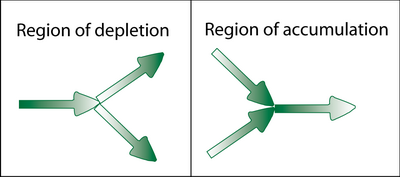
∂C/∂t < 0: mass depletion occurs and voids form (positive flux divergence)
∂C/∂t > 0: mass accumulates in growths – hillocks and whiskers (negative flux divergence)
∂C/∂t = 0: there is no change in atomic concentration and no damage occurs.
All the metal parts through which current flows in integrated circuits are potentially susceptible to electromigration effects. Different aspects are important in interconnects, contacts and vias.
As an added complication, the system observed is never static. Interactions within the metallization line result in the:
- movement of grain boundaries (grain growth)
- induction of heating
- recrystallization of the grain structure
- subtle evolution of microstructure and chemical composition.
The main contributions to flux divergence within metallization lines are: variations in microstructure, material or temperature.
Variation in Microstructure
Grain boundaries within Al-based metallization lines act as fast diffusion paths compared to the bulk system. The atomic environment at a boundary is less confining and contains fewer obstacles to diffusion. Accordingly, the activation energy for grain boundary diffusion is lower than that for bulk diffusion. As diffusion at grain boundaries far exceeds transport through the bulk of grains, the overall rate of atomic transport is greatly affected by the grain size, which determines the area of grain boundary in a given volume of sample.
The grain structure within metallization lines can vary from place to place: for example, the deposition technique would affect the degree of variation of microstructure. The associated property variations also lead to electromigration damage. Differences in microstructure or properties can be very large or barely perceptible, involving variations in grain orientation, grain size, chemical composition, atomic diffusivity, effective valency and vacancy generation within the grain structure.
Electromigration-induced damage is profoundly affected by grain structure: for example single-crystal aluminium stripes exhibit “infinite” life. This is because atomic diffusion and drift, for a metallization based on Al, are dominated by transport along grain boundaries rather than transport through the bulk of grains.
Some examples of microstructural variations are:-
Triple points
A film with a uniform grain size has a network of grain boundaries meeting at triple points (strictly, triple lines in 3-D). In annealed thin films it is usual for the grain structure to be in a 2-D pattern, with each grain occupying the full thickness of the film.
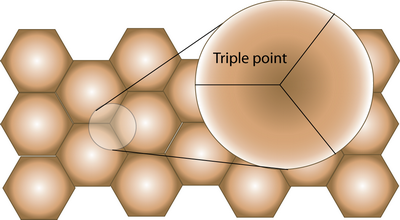
For a common metallization, such as Al-Cu, where the migrating atoms are solely confined to grain boundaries, it is possible to get divergences in mass transport at the triple points found in interconnect and contact lines. The atomic diffusivity in a given boundary can vary widely, depending on the structure of the boundary, which is related to the crystallographic misorientation of the grains. But even if we assume that all the grain boundaries are high-angle boundaries with similar diffusivities, it can easily be understood that flux divergences must arise at triple points.
When the direction of migration is such that one grain boundary leads into and two boundaries lead away from a triple point, the negative flux divergence can lead to the formation of a void. The converse is true when two boundaries lead into a triple point and one leaves, giving mass accumulation and possible hillock formation.
It would be assumed that a metallization line consisting of numerous triple points would be full of defects. This is not the case, as described by the concept known as the Blech length. Often, no damage is observed at triple points because they are closer than this critical length for damage e.g. for a current density of 1 x 10⁹ A m2, a line length of several hundred micrometers will not be susceptible to electromigration. A longer metallization line would have a larger number of triple points and hence an increased likelihood of this kind of failure. However, other factors come into effect as metallization line length increases, thus resulting in yet further damage.
Differences in grain size
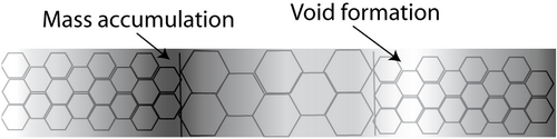
A fine-grained region contains more grain boundaries for atomic migration, than a coarse-grained region. Accumulation of atoms therefore occurs when atomic migration is from a fine-grained region moving into a coarser grained region. Conversely, voiding occurs when the migration is from a coarse to a finer grain size.
To avoid damage-inducing mass divergences, a bamboo-like grain structure (as shown in the SEM micrograph below) is desirable. The lack of continuous grain boundary paths for diffusion results in negligible mass transport along grain boundaries. The driving force for electromigration is predominantly perpendicular to the grain boundaries.
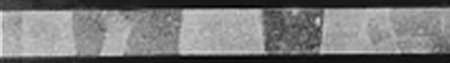
SEM micrograph of a metallization line containing a bamboo structure - grain boundaries are perpendicular to electron flow. (Reprinted with permission from: A.G. Domenicucci et.al: Effect of copper on the microstructure and electromigration lifetime Ti-AlCu-Ti fine lines in the presence of tungsten diffusion barriers. J. Appl. Phys. 80, p4952. Copyright 1998. American Institute of Physics.)
The animation below shows bamboo structure and its resistance to EM-damage.
Variations in Material
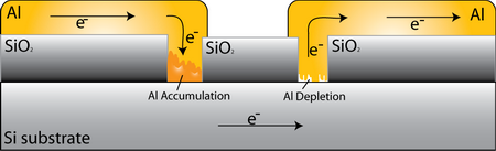
Different materials are used within an integrated circuit: for example, the Si substrate, W vias and Al interconnects. Differences in diffusion rates between two materials result in atomic flux divergence at the interface between them.
If the current flows from a material with a higher diffusivity to one with a lower diffusivity, the interface between the materials is a region of mass accumulation. Conversely when current flows from material with a lower diffusivity to another material with a higher diffusivity, void formation takes place at the interface. Electromigration-induced damage is most evident where the change in diffusivity is very large, e.g. at a Cu/barrier interface or an Al line/ W via interface.
Two main examples of this can be seen in: contacts and vias.
Contacts
When current flows through the contacts, electromigration causes metal atoms to move away from and towards the semiconductor interface. The inability to replenish metal that has been removed from and the inability to remove metal brought to the semiconductor interface results in a region of mass divergence. At the contact window either accumulation or depletion of Al occurs, depending on the direction of current flow.
Vias
The IC architecture requires use of successive interconnect levels and therefore of vias that enable current to flow between the layers. For Al-based metallization, W plug vias are commonly employed due to their high reliability, though structures consisting of Al-Cu vias can be used but are more difficult to make. As Al metallization tends to migrate whilst W exhibits negligible atomic transport (as shown in values of self-diffusion below), via-interconnect interfaces become sites of potentially large mass divergences.
The bulk lattice diffusivity values of Al and W at 300 K (assumed service temperature of the IC) are*:
DAl, bulk = 3.2×10⁻²⁹ m2 s-1
0 < DW, bulk < 5×10-88 m2 s-1 (negligible)
*Values calculated from data in Smithells Metals Reference Book, 6th Ed., Mechanisms of Diffusion p.13-11; E.A. Brandes (editor), Butterworths, London (UK), 1983.
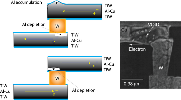
Source of SEM image of void formation at a via; R. Rosenberg et. al.: Copper metallization for high performance silicon technology, Annu. Rev. Mater. Sci. 20 p.229, 2000.
Degradation at vias is dependent not only on composition and grain structure, but also on the direction of current flow. The two modes of electromigration damage are shown above (in a schematic form and from an SEM micrograph). Voids form where the electrons flow away from the via, while a hillock forms when electrons flow towards the via.
In addition, thinned metal conductors and corners induce excessive Joule-heating effects and current crowding that lead to accelerated degradation.
Variations in Temperature
Temperature differences along the metallization line cause flux divergence because the diffusion coefficient is dependent on temperature. At higher temperatures, diffusion rates are increased. If there is a variation of temperature along the metal line, regions of accumulation and void growth would develop over time. Although the silicon substrate acts as a very good heat sink, the temperature along a line can vary because of heat generation in the underlying semiconductor components and because of local heating due to current crowding in the metallization itself.