
3.4.7: Models
- Page ID
- 89974

A second, and some people think more accurate, way to find \(V_{t}\) is to look at the characteristics of the MOS transistor in its linear regime. The test circuit looks like what you see in Figure \(\PageIndex{1}\). In this case, \(V_{\text{ds}}\) is kept quite small (0.2 Volts or so) and the gate voltage \(V_{\text{gs}}\) is swept over some range. If you look back at this equation in another module, we can slightly re-write it to see that \[I_{d} = \frac{\mu_{s} c_{\text{ox}} W V_{\text{ds}}}{L} \left(V_{\text{gs}} - V_{t}\right) \]
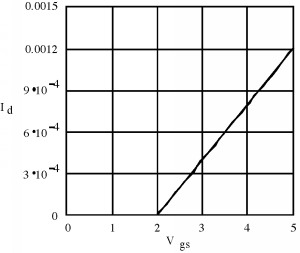
This equation will obviously give us a linear plot of \(I_{d}\) as a function of \(V_{\text{gs}}\), which will look something like Figure \(\PageIndex{2}\). Obviously, this is a device with a threshold voltage of about 2 volts. Can you figure out what \(k\) is for this transistor? If not, go back and re-read some stuff.
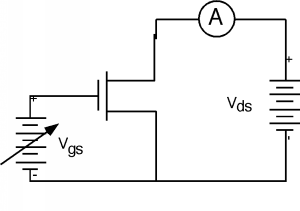
Figure \(\PageIndex{1}\): Circuit for finding \(V_{t}\)
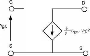
Now let's address a fundamental question concerning all of this: So what? What do we have here? One answer is that we have another device which in some way looks like the bipolar transistor we studied in the last chapter. In the saturation regime, the device looks and acts like a current source, and could probably be used as an amplifier. It is pretty easy to make a small signal model. The drain acts like a current source, which is controlled by \(V_{\text{gs}}\). What should we do about the gate terminal? The gate really is not connected to anything inside the transistor, so it looks just like an open circuit. (In fact, there is a capacitance \(C_{\text{gate}} = c_{\text{ox}} A_{\text{gate}}\) where \(A_{\text{gate}} = WL\), the area of the gate, but in most low frequency linear applications, this capacitance is not significant.) Thus our small signal model for the MOSFET, if it is operating in it saturation mode, is as seen in Figure \(\PageIndex{3}\).
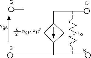
This seems to be a pretty good amplifier. It has infinite input impedance (and hence will not load down the previous stage of the amplifier) and it has a nice (but non-linear) voltage controlled current source for its output. A figure in the section on MOS regimes shows that as \(V_{\text{ds}}\) is increased, the channel length does, in fact, get a bit shorter. The increased \(V_{\text{ds}}\) makes the pinch-off region expand a bit, which, of course, robs from the channel region. A shorter channel means slightly less channel resistance, and so \(I_{d}\) actually increases a bit with increasing \(V_{\text{ds}}\) instead of staying constant. We saw from the bipolar transistor, that when this occurs, we must add a resistor in parallel with our current source. Thus, let's complete the model with an additional \(r_{o}\) but in fact, we will put it in with a dashed line, because except for very short channel devices, it has very little effect on device performance (Figure \(\PageIndex{4}\)).
The MOSFET has several advantages over the bipolar transistor. One of the main ones, as we shall see, is that it is much easier to make. You only need two n-regions in a single p-type substrate. It is basically a surface device. This means you do not have to pile up different layers of n and p type material as you do with the bipolar transistor. Finally, we shall see that a variation on the MOSFET technology offers a huge advantage over bipolar devices when it comes to building logic circuits with a large number of gates (VLSI and ULSI circuits).
To see why this is so, we have to digress for just a little bit, and discuss logic circuits.