
3.5: MOS Regimes
- Page ID
- 88537

\( \newcommand{\vecs}[1]{\overset { \scriptstyle \rightharpoonup} {\mathbf{#1}} } \)
\( \newcommand{\vecd}[1]{\overset{-\!-\!\rightharpoonup}{\vphantom{a}\smash {#1}}} \)
\( \newcommand{\dsum}{\displaystyle\sum\limits} \)
\( \newcommand{\dint}{\displaystyle\int\limits} \)
\( \newcommand{\dlim}{\displaystyle\lim\limits} \)
\( \newcommand{\id}{\mathrm{id}}\) \( \newcommand{\Span}{\mathrm{span}}\)
( \newcommand{\kernel}{\mathrm{null}\,}\) \( \newcommand{\range}{\mathrm{range}\,}\)
\( \newcommand{\RealPart}{\mathrm{Re}}\) \( \newcommand{\ImaginaryPart}{\mathrm{Im}}\)
\( \newcommand{\Argument}{\mathrm{Arg}}\) \( \newcommand{\norm}[1]{\| #1 \|}\)
\( \newcommand{\inner}[2]{\langle #1, #2 \rangle}\)
\( \newcommand{\Span}{\mathrm{span}}\)
\( \newcommand{\id}{\mathrm{id}}\)
\( \newcommand{\Span}{\mathrm{span}}\)
\( \newcommand{\kernel}{\mathrm{null}\,}\)
\( \newcommand{\range}{\mathrm{range}\,}\)
\( \newcommand{\RealPart}{\mathrm{Re}}\)
\( \newcommand{\ImaginaryPart}{\mathrm{Im}}\)
\( \newcommand{\Argument}{\mathrm{Arg}}\)
\( \newcommand{\norm}[1]{\| #1 \|}\)
\( \newcommand{\inner}[2]{\langle #1, #2 \rangle}\)
\( \newcommand{\Span}{\mathrm{span}}\) \( \newcommand{\AA}{\unicode[.8,0]{x212B}}\)
\( \newcommand{\vectorA}[1]{\vec{#1}} % arrow\)
\( \newcommand{\vectorAt}[1]{\vec{\text{#1}}} % arrow\)
\( \newcommand{\vectorB}[1]{\overset { \scriptstyle \rightharpoonup} {\mathbf{#1}} } \)
\( \newcommand{\vectorC}[1]{\textbf{#1}} \)
\( \newcommand{\vectorD}[1]{\overrightarrow{#1}} \)
\( \newcommand{\vectorDt}[1]{\overrightarrow{\text{#1}}} \)
\( \newcommand{\vectE}[1]{\overset{-\!-\!\rightharpoonup}{\vphantom{a}\smash{\mathbf {#1}}}} \)
\( \newcommand{\vecs}[1]{\overset { \scriptstyle \rightharpoonup} {\mathbf{#1}} } \)
\(\newcommand{\longvect}{\overrightarrow}\)
\( \newcommand{\vecd}[1]{\overset{-\!-\!\rightharpoonup}{\vphantom{a}\smash {#1}}} \)
\(\newcommand{\avec}{\mathbf a}\) \(\newcommand{\bvec}{\mathbf b}\) \(\newcommand{\cvec}{\mathbf c}\) \(\newcommand{\dvec}{\mathbf d}\) \(\newcommand{\dtil}{\widetilde{\mathbf d}}\) \(\newcommand{\evec}{\mathbf e}\) \(\newcommand{\fvec}{\mathbf f}\) \(\newcommand{\nvec}{\mathbf n}\) \(\newcommand{\pvec}{\mathbf p}\) \(\newcommand{\qvec}{\mathbf q}\) \(\newcommand{\svec}{\mathbf s}\) \(\newcommand{\tvec}{\mathbf t}\) \(\newcommand{\uvec}{\mathbf u}\) \(\newcommand{\vvec}{\mathbf v}\) \(\newcommand{\wvec}{\mathbf w}\) \(\newcommand{\xvec}{\mathbf x}\) \(\newcommand{\yvec}{\mathbf y}\) \(\newcommand{\zvec}{\mathbf z}\) \(\newcommand{\rvec}{\mathbf r}\) \(\newcommand{\mvec}{\mathbf m}\) \(\newcommand{\zerovec}{\mathbf 0}\) \(\newcommand{\onevec}{\mathbf 1}\) \(\newcommand{\real}{\mathbb R}\) \(\newcommand{\twovec}[2]{\left[\begin{array}{r}#1 \\ #2 \end{array}\right]}\) \(\newcommand{\ctwovec}[2]{\left[\begin{array}{c}#1 \\ #2 \end{array}\right]}\) \(\newcommand{\threevec}[3]{\left[\begin{array}{r}#1 \\ #2 \\ #3 \end{array}\right]}\) \(\newcommand{\cthreevec}[3]{\left[\begin{array}{c}#1 \\ #2 \\ #3 \end{array}\right]}\) \(\newcommand{\fourvec}[4]{\left[\begin{array}{r}#1 \\ #2 \\ #3 \\ #4 \end{array}\right]}\) \(\newcommand{\cfourvec}[4]{\left[\begin{array}{c}#1 \\ #2 \\ #3 \\ #4 \end{array}\right]}\) \(\newcommand{\fivevec}[5]{\left[\begin{array}{r}#1 \\ #2 \\ #3 \\ #4 \\ #5 \\ \end{array}\right]}\) \(\newcommand{\cfivevec}[5]{\left[\begin{array}{c}#1 \\ #2 \\ #3 \\ #4 \\ #5 \\ \end{array}\right]}\) \(\newcommand{\mattwo}[4]{\left[\begin{array}{rr}#1 \amp #2 \\ #3 \amp #4 \\ \end{array}\right]}\) \(\newcommand{\laspan}[1]{\text{Span}\{#1\}}\) \(\newcommand{\bcal}{\cal B}\) \(\newcommand{\ccal}{\cal C}\) \(\newcommand{\scal}{\cal S}\) \(\newcommand{\wcal}{\cal W}\) \(\newcommand{\ecal}{\cal E}\) \(\newcommand{\coords}[2]{\left\{#1\right\}_{#2}}\) \(\newcommand{\gray}[1]{\color{gray}{#1}}\) \(\newcommand{\lgray}[1]{\color{lightgray}{#1}}\) \(\newcommand{\rank}{\operatorname{rank}}\) \(\newcommand{\row}{\text{Row}}\) \(\newcommand{\col}{\text{Col}}\) \(\renewcommand{\row}{\text{Row}}\) \(\newcommand{\nul}{\text{Nul}}\) \(\newcommand{\var}{\text{Var}}\) \(\newcommand{\corr}{\text{corr}}\) \(\newcommand{\len}[1]{\left|#1\right|}\) \(\newcommand{\bbar}{\overline{\bvec}}\) \(\newcommand{\bhat}{\widehat{\bvec}}\) \(\newcommand{\bperp}{\bvec^\perp}\) \(\newcommand{\xhat}{\widehat{\xvec}}\) \(\newcommand{\vhat}{\widehat{\vvec}}\) \(\newcommand{\uhat}{\widehat{\uvec}}\) \(\newcommand{\what}{\widehat{\wvec}}\) \(\newcommand{\Sighat}{\widehat{\Sigma}}\) \(\newcommand{\lt}{<}\) \(\newcommand{\gt}{>}\) \(\newcommand{\amp}{&}\) \(\definecolor{fillinmathshade}{gray}{0.9}\)The final equation of Section 3.4 looks a lot like the \(I \text{-} V\) characteristics of a resistor! \(I_{d}\) is simply proportional to the drain voltage \(V_{\text{ds}}\). The proportionality constant depends on the dimensions of the device, \(W\) and \(L\), as they intuitively should. The current increases as the transistor gets wider; it decreases as the transistor gets longer. It also depends on \(c_{\text{ox}}\) and \(\mu_{s}\), and on the difference between the gate voltage and the threshold voltage \(V_{T}\). Note that if we adjust \(V_{\text{gs}}\) we can change the slope of the \(I \text{-} V\) curve. We have made a voltage-controlled resistor!
Figure \(\PageIndex{1}\): The MOSFET \(I\text{-}V\) graph in the linear regime
Caution is advised with this result, however, because we have overlooked something quite important. Let's go back to our picture of the gate and the batteries involved in the operation of the MOS transistor. Here we have explicitly shown the channel as a black band and we have introduced a new quantity, \(V_{c} (x)\), the voltage along the channel, and a coordinate \(x\), which tells us where we are on the channel relative to the source and drain. Note that once we apply a drain source potential, \(V_{\text{ds}}\), the potential in the channel \(V_{c} (x)\) changes with distance along the channel. At the source end, \(V_{c}(0) = 0\) as the source is grounded. At the drain end, \(V_{c}(L) = V_{\text{ds}}\). We will define a voltage \(V_{\text{gc}}\), which is the potential difference between the gate voltage and the voltage in the channel. \[V_{\text{gc}} (x) \equiv V_{\text{gs}} - V_{c} (x)\]
Thus, \(V_{\text{gc}}\) goes from \(V_{\text{gs}}\) at the source end to \(V_{\text{gs}} - V_{\text{ds}}\)at the drain end.
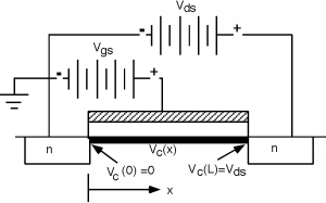
Figure \(\PageIndex{2}\): Effect of \(V_{\text{ds}}\) on channel potential
The net charge density in the channel depends upon the potential difference between the gate and the channel at each point along the channel, not just \(V_{\text{gs}} - V_{T}\). Thus we have to modify the equation of another module to take this into account. \[\begin{array}{l} Q_{\text{chan}} &= c_{\text{ox}} \left(V_{\text{gc}} (x) - V_{T}\right) \\ &= c_{\text{ox}} \left(V_{\text{gs}} - V_{c} (x) - V_{T}\right) \end{array}\]
This, in turn, modifies the integral relation between \(I_{d}\) and \(V_{\text{gs}}\). \[\int\limits_{0}^{V_{\text{ds}}} \mu_{s} c_{\text{ox}} \left(V_{\text{gs}} - V_{T} - V_{c}(x) \right) W \ dV_{c} (x) = \int\limits_{0}^{L} I_{d} \ dx\]
Equation \(\PageIndex{3}\) is only slightly harder to integrate than the one before, and we get for the drain current \[I_{d} = \frac{\mu_{s} c_{\text{ox}} W}{L} \left( \left(V_{\text{gs}}-V_{T}\right) V_{\text{ds}} - \frac{V_{\text{ds}}{ }^2}{2} \right)\]
This equation is called the Sah Equation after C.T. Sah, who first described the MOS transistor operation this way back in 1964. It is very important because it describes the basic behavior of the MOS transistor.
Note that for small values of \(V_{\text{ds}}\), a previous equation and Equation \(\PageIndex{4}\) will give us the same \(I_{d} \text{-} V_{\text{ds}}\) behavior, because we can ignore the \(V_{\text{ds}}{ }^2\) term in Equation \(\PageIndex{4}\). This is called the linear regime because we have a straight-line relationship between the drain current and the drain-source voltage. As \(V_{\text{ds}}\) starts to get larger however, the squared term will begin to kick in and the plot will start to curve over. Obviously, something is causing the current to drop off as \(V_{\text{ds}}\) gets larger. This is because the voltage difference between the gate and the channel is becoming less, which means there is less charge in the channel to provide conduction. We can graphically show this by making the channel layer look thinner as we move from the source to the drain. Equation \(\PageIndex{4}\), and in fact, Figure \(\PageIndex{3}\) would make us think that if \(V_{\text{ds}}\) gets large enough, that the drain current \(I_{d}\) should actually start decreasing again, and maybe even become negative! This does not seem very intuitive, so let's take a look in more detail at the place where \(I_{d}\) becomes a maximum. We can define \(V_{\text{d sat}}\) as the source-drain voltage where \(I_{d}\) becomes a maximum. We can find this by taking the derivative of \(I_{d}\) with respect to \(V_{\text{ds}}\) and setting the derivative to \(0\). \[\begin{array}{l} \frac{d}{d V_{\text{ds}}} \left(I_{d}\right) &= 0 \\ &= \frac{\mu_{s} c_{\text{ox}} W}{L} \left(V_{\text{gs}} - V_{T} - V_{\text{d sat}} \right) \end{array}\]
On dropping constants: \[V_{\text{d sat}} = V_{\text{gs}} - V_{T}\]
Rearranging this equation gives us a little more insight into what is going on. \[\begin{array}{l} V_{\text{gs}} - V_{\text{d sat}} &= V_{T} \\ &= V_{\text{gc}} (L) \end{array}\]
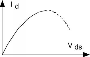
Figure \(\PageIndex{3}\): \(I\text{-}V\) characteristics showing turn-over
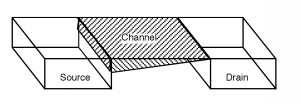
Figure \(\PageIndex{4}\): Effect of \(V_{\text{ds}}\) on the channel
At the drain end of the channel, when \(V_{\text{ds}}\) just equals \(V_{\text{d sat}}\), the difference between the gate voltage and the channel voltage, \(V_{\text{gc}} (L)\) is just equal to \(V_{T}\), the threshold voltage. Any further increase in \(V_{\text{ds}}\) and the difference between the gate and the channel (in the channel region just near the drain) will drop below the threshold voltage. This means that when \(V_{\text{ds}}\) gets bigger than \(V_{\text{d sat}}\), the channel just near the drain region disappears! We no longer have sufficient voltage between the gate and the channel region to maintain an inversion layer, so we simply revert to a depletion condition. This is called pinch off, as seen in Figure \(\PageIndex{5}\).
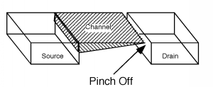
Figure \(\PageIndex{5}\): Channel in pinch-off
What happens to the drain current when we hit pinch off? It looks like it might go to zero, but that is not the right answer! Although there is no active channel in the pinch-off region, there is still silicon — it just happens to be depleted of all free carriers. There is an electric field going from the drain to the channel, and any electrons which move along the channel to the pinch-off region are sucked across by the field, and enter the drain. This is just like the current that flows in the reverse saturation condition of a diode. There are no free carriers in the depletion region of the diode, yet \(I_{\text{sat}}\) does flow across the junction region.
Under pinch-off conditions, further increases in \(V_{\text{ds}}\), does not result in more drain current. You can think of the pinched-off channel as a resistor, with a voltage of \(V_{\text{d sat}}\) across it. When \(V_{\text{ds}}\) gets bigger than \(V_{\text{d sat}}\), the excess voltage appears across the pinch-off region, and the voltage across the channel remains fixed at \(V_{\text{d sat}}\). If the channel keeps the same charge, and has the same voltage across it, then the current through the channel (and into the drain) will remain fixed, at a value we will call \(I_{\text{d sat}}\).
There is one other figure which sometimes helps in seeing what is going on. We will plot potential energy for an electron, as it traverses across the channel. Since the source is at zero potential and the drain is at \(V_{\text{ds}}\), an electron will loose potential energy as it flows from the source to the drain. Figure \(\PageIndex{6}\) shows some examples for various values of \(V_{\text{ds}}\):
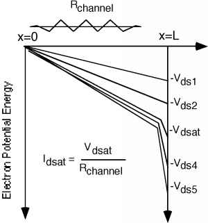
For the first two drain voltages, \(V_{\text{ds}1}\) and \(V_{\text{ds}2}\), we are below pinch-off, and so the voltage drop across \(R_{\text{channel}}\) increases as \(R_{\text{channel}}\) increases, and hence, so does \(I_{d}\). At \(V_{\text{d sat}}\), we have just reached pinch-off, and we are starting to see the "high field" depletion region begin to develop. Since electric field is just the derivative of the potential, the slope of curves in Figure \(\PageIndex{6}\) gives you an idea of how big the electric field will be. For further increases in \(V_{\text{ds}}\), such as \(V_{\text{ds}4}\) and \(V_{\text{ds}5}\) all of the additional voltage just shows up as a high field drop at the end of the channel. The voltage drop across the conducting part of the channel stays fixed (more or less) at \(V_{\text{d sat}}\) and so the drain current stays more or less fixed at \(I_{\text{d sat}}\). Substituting the expression for \(V_{\text{sat}}\) into the expression for \(I_{d}\), we can get an expression for \(I_{\text{d sat}}\): \[I_{\text{d sat}} = \frac{\mu_{s} c_{\text{ox}} W}{2L} \left(V_{\text{gs}} - V_{T}\right)^{2}\]
We can define a new constant, \(k\), where \[k = \frac{\mu_{s} c_{\text{ox}} W}{L}\]
So that \[I_{\text{d sat}} = \frac{k}{2} \left(V_{\text{gs}} - V_{T}\right)^{2}\]
What this means for Figure \(\PageIndex{3}\) is that when \(V_{\text{ds}}\) gets to \(V_{\text{d sat}}\), we simply hold \(I_{d}\) fixed from then on, with a value of \(I_{\text{d sat}}\). For different values of \(V_{g}\), the gate voltage, we are going to have a different \(I_{d} \text{-} V_{\text{ds}}\) curve, and so once again, we end up with a family of "characteristic curves" for the MOSFET. These are shown in Figure \(\PageIndex{8}\).
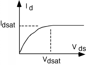
Figure \(\PageIndex{7}\): Complete \(I\text{-}V\) curve for the MOSFET
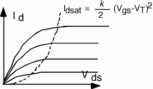
Figure \(\PageIndex{8}\): Characteristic curves for a MOSFET
This also gives us a fairly easy way in which to "sketch" a set of characteristic curves for a given device. Suppose we have a MOS field effect transistor which has a threshold voltage of 2 volts, a width of 10 microns, and a channel length of 1 micron, an oxide thickness of 150 angstroms, and a surface mobility of \(400 \ \frac{\mathrm{C}}{\mathrm{V} \cdot \mathrm{sec}}\). Using \(\varepsilon_{\text{ox}} = 3.3 \times 10^{-13} \ \frac{\mathrm{F}}{\mathrm{cm}}\), we get a value of \(2.2 \times 10^{-7} \ \frac{\mathrm{F}}{\mathrm{C}}\) for \(c_{\text{ox}}\). This then makes \(k\) have a value of \[\begin{array}{l} k &= \frac{\mu_{s} c_{\text{ox}} W}{L} \\ &= \frac{400 \cdot 2.2 \times 10^{-7} \cdot 10}{1} \\ &= 8.8 \times 10^{-4} \ \frac{\mathrm{amp}}{\mathrm{volt}^2} \end{array}\]