
3.4.4: MOS Transistor
- Page ID
- 89971

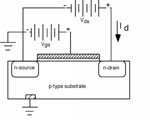
Now we can go back now to our initial structure, shown in the introduction to MOSFETs, only this time we will add an oxide layer, a gate structure, and another battery so that we can invert the region under the gate and connect the two n-regions together. We'll also identify some names for parts of the structure, so we will know what we are talking about. For reasons which will be clear later, we call the n-region connected to the negative side of the battery the source, and the other one the drain. We will ground the source, and also the p-type substrate. We add two batteries: \(V_{\text{gs}}\) between the gate and the source, and \(V_{\text{ds}}\) between the drain and the source.
It will be helpful if we also make another sketch which gives us a perspective view of the device. For this we strip off the gate and oxide, but we will imagine that we have applied a voltage greater than \(V_{t}\) to the gate, so there is a n-type region called the channel which connects the two. We will assume that the channel region has length \(L\) and width \(W\), as shown in Figure \(\PageIndex{2}\).
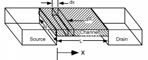
Next we want to take a look at a little section of channel, and find its resistance \(dR\), when the little section is \(dx\) long. \[dR = \frac{dx}{\sigma_{s} W}\]
We have introduced a slightly different form for our resistance formula here. Normally, we would have a simple \(\sigma\) in the denominator, and an area \(A\) for the cross-sectional area of the channel. It turns out to be very hard to figure out what that cross sectional area of the channel is, however. The electrons which form the inversion layer crowd into a very thin sheet of surface charge which really has little or no thickness, or penetration into the substrate.
If, on the other hand we consider a surface conductivity (units of \(\mathrm{mhos} = \mho = \Omega^{-1}\)), \(\sigma_{s}\), where \[\sigma_{s} = \mu_{s} Q_{\text{chan}}\]
then we will have an expression which we can evaluate. Here, \(mu_{s}\) is a surface mobility, with units of \(\frac{\mathrm{cm}^2}{\mathrm{V} \cdot \mathrm{sec}}\). We ran into \(\mu\) in earlier chapters, when we were building our simple conduction model. It was the quantity which represented the proportionality between the average carrier velocity and the electric field. \[\bar{v} = \mu E\] \[\mu = \frac{q \tau}{m}\]
The surface mobility is a quantity which has to be measured for a given system, and is usually just a number which is given to you. Something around \(300 \ \frac{\mathrm{cm}^2}{\mathrm{V} \cdot \mathrm{sec}}\) is about right for silicon. \(Q_{\text{chan}}\) is called the surface charge density or channel charge density and it has units of \(\frac{\mathrm{Coulombs}}{\mathrm{cm}^2}\). This is like a sheet of charge, which is different from the bulk charge density, which has units of \(\frac{\mathrm{Coulombs}}{\mathrm{cm}^2}\). Note that: \[\begin{array}{l} \frac{\mathrm{cm}^2}{\mathrm{Volt} \cdot \mathrm{sec}} \frac{\mathrm{Coulombs}}{\mathrm{cm}^2} &= \frac{\frac{\mathrm{Coul}}{\mathrm{sec}}}{\mathrm{Volt}} \\ &= \frac{I}{V} \\ &= \mho \end{array}\]
It turns out that it is pretty simple to get an expression for \(Q_{\text{chan}}\), the surface charge density in the channel. For any given gate voltage \(V_{\text{gs}}\), we know that the charge density on the gate is given simply as: \[Q_{g} = c_{\text{ox}} V_{\text{gs}}\]
However, until the gate voltage \(V_{\text{gs}}\) gets larger than \(V_{t}\) we are not creating any mobile electrons under the gate, we are just building up a depletion region. We'll define \(Q_{T}\) as the charge on the gate necessary to get to threshold. \(Q_{T} = c_{\text{ox}} V_{t}\). Any charge added to the gate above \(Q_{T}\) is matched by charge \(Q_{\text{chan}}\) in the channel. Thus, it is easy to say: \[Q_{\text{chan}} = Q_{g} - Q_{T}\]
or \[Q_{\text{chan}} = c_{\text{ox}} \left(V_{g} - V_{t}\right)\]
Thus, putting Equation \(\PageIndex{8}\) and Equation \(\PageIndex{2}\) into Equation \(\PageIndex{1}\), we get: \[d(R) = \frac{d(x)}{\mu_{s} c_{\text{ox}} \left(V_{\text{gs}} - V_{t}\right) W}\]
If you look back at Figure \(\PageIndex{1}\), you will see that we have defined a current \(I_{d}\) flowing into the drain. That current flows through the channel, and hence through our little incremental resistance \(dR\), creating a voltage drop \(d \left(V_{c}\right)\) across it, where \(V_{c}\) is the channel voltage. \[\begin{array}{l} d \left(V_{c} (x)\right) &= I_{d} d(R) \\ &= \frac{I_{d} d(x)}{\mu_{s} c_{\text{ox}} \left(V_{\text{gs}} - V_{t}\right) W} \end{array}\]
Let's move the denominator to the left, and integrate. We want to do our integral completely along the channel. The voltage on the channel \(V_{c} (x)\) goes from \(0\) on the left to \(V_{\text{ds}}\) on the right. At the same time, \(x\) is going from \(0\) to \(L\). Thus our limits of integration will be \(0\) and \(V_{\text{ds}}\) for the voltage integral of \(d \left(V_{c} (x)\right)\) and from \(0\) to \(L\) for the integral of \(dx\). \[\int\limits_{0}^{V_{\text{ds}}} \mu_{s} c_{\text{ox}} \left(V_{\text{gs}} - V_{t}\right) W \ d V_{c} = \int\limits_{0}^{L} I_{d} \ dx\]
Both integrals are pretty trivial. Let's swap the equation order, since we usually want \(I_{d}\) as a function of applied voltages. \[I_{d} L = \mu_{s} c_{\text{ox}} W \left(V_{\text{gs}} - V_{t}\right) V_{\text{ds}}\]
We now simply divide both sides by \(L\), and we end up with an expression for the drain current \(I_{d}\) in terms of the drain-source voltage \(V_{\text{ds}}\), the gate voltage \(V_{\text{gs}}\), and some physical attributes of the MOS transistor. \[I_{d} = \left(\frac{\mu_{s} c_{\text{ox}} W}{L} \left(V_{gs} - V_{t}\right) \right) V_{ds}\]