
4.4: Load and Store Architecture
- Page ID
- 76112

4.4.1 Load and Store CPU
When designing a CPU, there are two basic ways that the CPU can access memory. The CPU can allow direct access memory as part of any instruction, or only allow memory to be accessed with special instructions called load and store instructions. A CPU that allows any instruction to access memory normally has instructions that vary in length and requires the CPU to spend multiple clock cycles decoding the instruction and accessing memory. This is more common with Complex Instruction Set Computers, or CISC architectures, such as the Intel x86 series of CPUs.
ARM is an example of another type of CPU, called a Reduced Instruction Set Computer, or RISC architecture. One of the major design criteria when creating a RISC CPU was that all the instructions would be regular, meaning the instructions would all be the same size and require the instructions use similar amounts of time for decoding and executing the instructions. This regularity of instructions allows the CPU to be run faster and to be optimized using techniques such as pipeline designs that are difficult, if not impossible, on an CISC computer. It also allows the compiler to take advantage of a smaller number of more regular instructions, rather than a large number of generic complex instructions. Being able to compile programs using behavior specific for a program rather than using generic complex instructions allows compilers to better optimize code, making programs faster.
RISC instruction set computers do not allow all instructions to access memory, but have special operations to load and store data to registers. All internal CPU units use registers for input and cannot access memory directly. External data in memory must first be loaded into a register before it can be used.
The CPU architecture illustrated in the following block diagram is the CPU architecture from Figure 11 with the load and store instructions added. This block diagram CPU is now a 3- address load and store architecture.

Figure 19: 3-address load and store CPU
Note that this diagram behaves exactly as the CPU in Figure 11 for any 3-address instruction; the changes between this CPU and the 3-address CPU only impact the new load and store commands. How the 3-address CPU maps into this new CPU is shown in the diagram below.
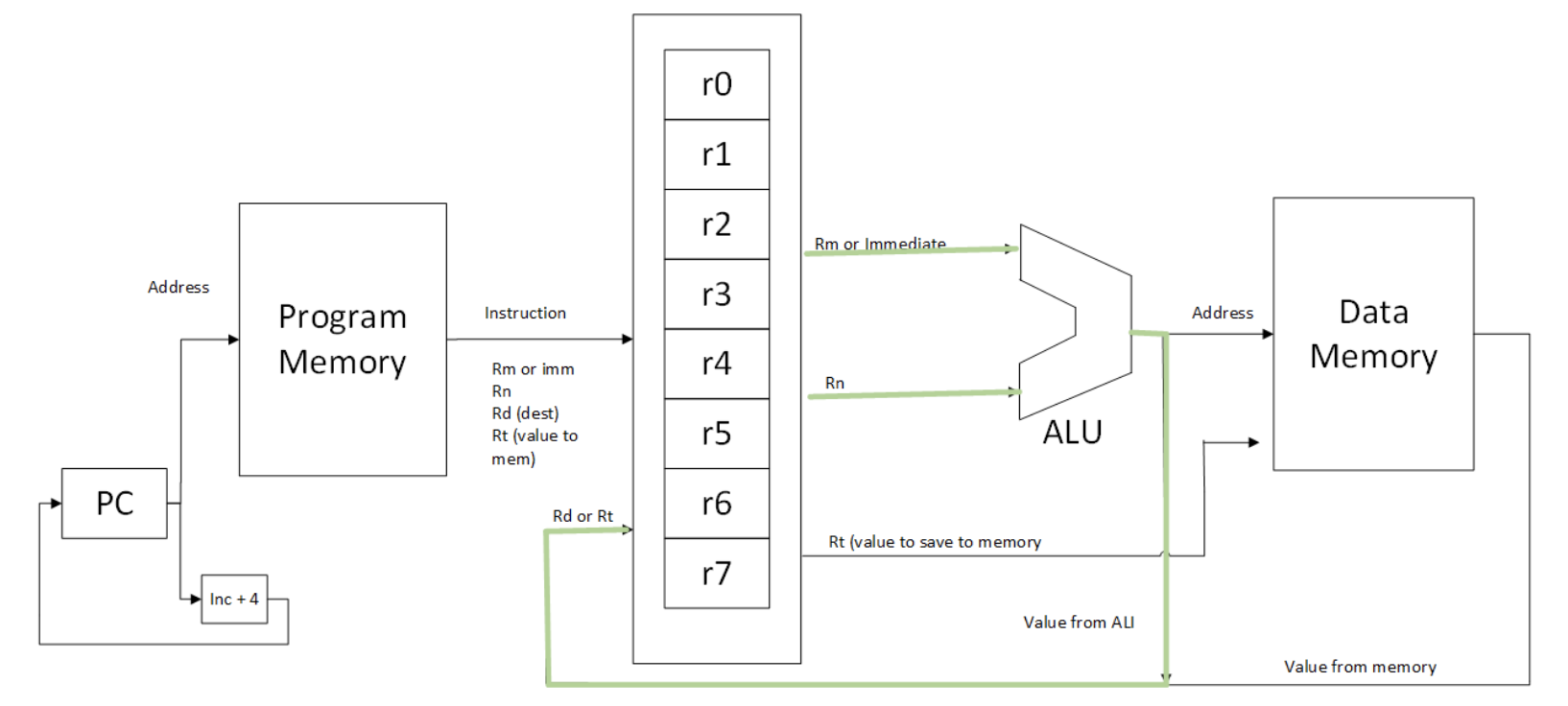
Figure 20: 3-address load and store CPU highlighting 3-address datapath
The changes for all the CPUs in this text will follow this strategy of allowing all previous programs to work, but enhancing the CPU to add new features. If you first identify how the previous CPU is manifested in the new diagram, it will be easier to understand than trying to take into account all of the complexity of the new diagram without a context.
Figure 20 shows that for 3-address instructions, the ALU still gets the same values from registers or immediate values, produces an output, and sends the output back to the Register Bank.
The changes in the new CPU are due to adding loading and storing of data from memory to a register. The operation for saving data to a register is illustrated in Figure 21.
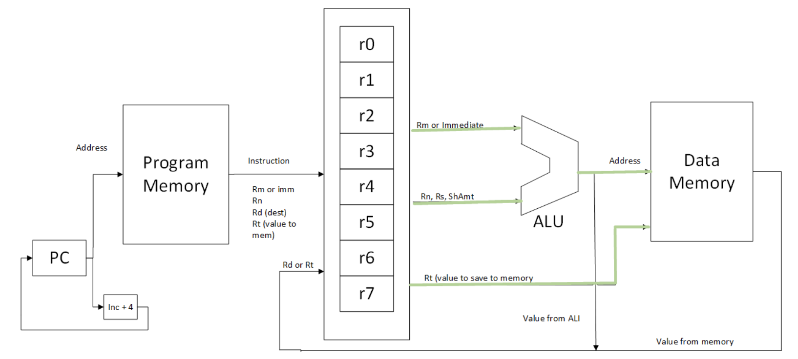
Figure 21: 3-address load and store CPU highlighting store operation
As shown in this diagram, the Rn register is added to either the Rm register or the immediate value to calculate a memory address from which to load the data and the data from the Rt register is put on the C bus to write to memory.
Next, figure 22 illustrates the loading data to the memory. As in Figure 21, the address is calculated in the ALU and passed to the data memory. The data memory reads the value at that address and places that value on the bus to send it back to the register bank. Note that this memory value is placed on the same bus as the output form the ALU. At the point where the results of the ALU and the result from a memory read collide a hardware component, called a multiplexer or MUX, will be inserted to choose which value to pass on to the register bank.
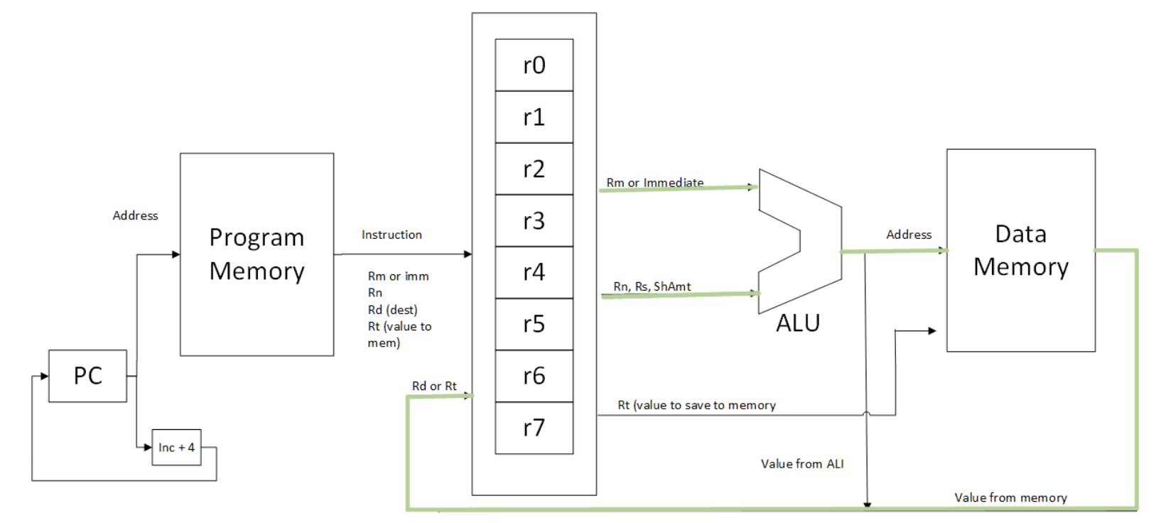
Figure 22: 3-address load and store CPU highlighting store operation
The instruction format for the LDR and Store Register (STR) instructions can add either an immediate or register value to the Rn value to calculate the memory address, so there are two formats for each instruction. The four formats are:
   LDR Rt, [Rn, immediate]
   LDR Rt, [Rn, Rm]
   STR Rt, [Rn, immediate]
   STR Rt, [Rn, Rm]
Examples of using these instructions are:
   LDR r1, [r2, #4]
   LDR r1, [r2, r3]
   STR r1, [r2, #4]
   STR r1, [r2, r3]
One very important detail about the immediate value in these instructions is that it is 12 bits, not the 8 bits that this CPU used to limit the value for immediate values in the Data Operations instructions.
The first LDR instruction adds the value representing a base memory address (in this case r2) to the immediate value in the address calculation (in this case #4) to produce the memory address of the value to load into r1. This statement says r1 ← M[r2 + 4].
The second LDR instruction adds the value representing a base memory address (in this case r2) to the register value in the address calculation (in this case r3) to produce the memory address of the value to load into r1. This statement says r1 ← M[r2 + r3].
The first STR instruction adds the value representing a base memory address (in this case r2) to the immediate value in the address calculation (in this case #4) to produce the memory address in which to store the value in r1. This statement says M[r2 + 4] ← r1.
The second STR instruction adds the value representing a base memory address (in this case r2) to the register value in the address calculation (in this case r3) to produce the memory address of the value to load into r1. This statement says M[r2 + r3] ← r1.
Note that there is a new register, Rt, which is r1 in both of the instructions above. Rt is different from other registers because for a LDR instruction it is the register to which the value retrieved from memory is stored and for the STR instruction it specifies the register value to store back to memory. Thus, it is given a separate designation from the other registers.
In addition, in the LDR and STR instructions the ALU no longer produces a value to be stored back to a register, but instead produces the address of a memory location from which to either read or store a value. For the LDR instruction the memory location is read and the value put on the bus is passed from the memory to registers.
For the STR instruction, the value to write to memory is read from register Rt and sent to the data input port on the Data Memory. The address of where to write the value in memory is produced by the ALU and sent to the data address port on the Data Memory and the value is written into memory at that address.
4.4.2 Auto incrementing of the Rt register
The ARM assembly language has a useful feature when executing load and store operations; it allows the Rn register to be automatically updated with the value that was calculated with the memory address used. This is called auto-incrementing the register. The following examples illustrates how to specify auto-incrementing.
No auto-incrementing:
      LDR r1, [r2, #4]
      STR r1, [r2, r3]
With no auto-incrementing, the value or r2 is not changed when executing a LDR or STR instruction.
Pre-incrementing
      LDR r1, [r2, #4]!
      STR r1, [r2, r3]!
With pre-incrementing, the value or r2 is changed before calculating the address, and the new address is used when executing a LDR or STR instruction.
Post-incrementing
      LDR r1, [r2], #4
      STR r1, [r2], r3
With post-incrementing, the value or r2 is changed after calculating the address, and the old address is used when executing a LDR or STR instruction.
4.4.3 Von Neumann vs Harvard Architecture
The next issue is whether or not a single memory exists that contains both text and data (Von Neumann architecture) or whether the memory is split between text and data segments (Harvard architecture). The ARM computer is a Von Neumann architecture and this can have a notable impact on the machine and executable code that is produced. However, the implementation of ARM memory allows the actual access of memory that can appear as if the memory is split between text and data. This means the ARM CPU can act like it has a Harvard architecture. This has a large impact on the CPU design, as the 3-address design in Figure 20 divides the memory into a text memory and an address memory. This has little impact in this chapter, but takes on an oversized importance in the actual implementation of the CPU.
4.4.4 Addressing modes in ARM assemblye
The previous section on the LDR and STR commands explained the format of the commands, but not how to use them in ARM assembly. This section will show the different addressing modes, or way to access variables, in ARM assembly. The addressing modes to be covered are immediate, direct, register direct, register indirect, register indirect with offset, indirect, and PC relative addressing.
Immediate Addressing
In immediate addressing the value to be used is included in the instruction itself. An example of immediate addressing is the following ADD instruction:
ADD r1, r2, #12
Note that an immediate value is very different than a constant. An immediate value is not stored in data memory, but is part of the instruction, so there is no need to load the value into a register before using it. A constant is a value stored in memory, like any other variable, except that its value cannot be changed. To use a constant, the value must be loaded into a register, which makes using a constant potentially more expensive to use than an immediate value.
Direct Addressing
With direct addressing, the address of a value is known. An example is when the value is stored at a label. Consider the following code fragment:
    LDR r1, =num
    LDR r1, [r1, #0]
    num: .word 5
In this code fragment, there is a known address of the value to be loaded. In this example, first the address of num (not the value 5) is loaded into register r1. The address in the register is then used to load the value into r1.
Register Direct
A value is a register direct if the value is stored in the register. In the following instruction, register direct addressing is used for both of addends.
ADD r1, r2, r3
Register Indirect
When using register indirect addressing, the address of the variable to use is stored in the register, and the value at that address is loaded into a register to be used later. This can be useful in a number of situations to access data. For example, the following would be an efficient way to access an array of integer data allocated beginning at the address of the label arr. In this case r1 will be incremented to the next element value as each array element value is loaded into r2.
    LDR r1, =arr
    LDR r2, [r1], #4
    .data
        arr: .word 10
Register Indirect with offset
Register indirect with offset addressing is the most efficient and effective way to handle addressing when there is a base address and values that are located at some known offset of that base. An example is structures or classes and will be used extensively later in this text when discussing the program stack. To see this, consider the following Java class:
    class A {
        long a;
        int b;
    }
For an address pointing to the start of the class in r1, the value for each variable can be loaded into r2 using the following instructions:
    LDR r2, [r1, #0]
    LDR r3, [r1, #8]
Indirect
Indirect addressing is like register indirect addressing except that the value in memory is actually an address to another value. In fact, the value that is addressed can be an address itself. For example, consider the following code fragment:
    LDR r1, =addr_num
    LDR r1, [r1, #0]
    LDR r1, [r1, #0]
.data
    num: .word 5
    addr_num: .word num
In this code fragment, the value at the address of label addr_num is the address of (reference to) the address of label num. To find the actual value, the address chain, or chain of references, must be traversed until the final value is found.
This becomes interesting because it gives an insight into the relationship between references and values. A value is simply the data at the address of a reference. References point to values and what the value is depends on its relationship.
This leads to the definition of two new terms: a reference type and a value type. A reference type implies that the value at the address is a reference to another value. A value type is a final value in the reference-value chain and is a value that is a program value.
PC relative
This is likely the most important type of addressing in ARM assembly. However, it requires that the concept of the PC be covered in some detail in Chapter 8. So, this type of addressing will be covered in detail as part of Chapter 8.