
2.3: Piezoelectric Devices
- Page ID
- 18945

Can we induce a material polarization in an insulator in a way that does not involve applying a voltage? If so, then this method can charge a capacitor, and we can discharge the capacitor as usual to produce electricity. Any device that accomplishes this task is an energy conversion device. Piezoelectric, pyroelectric, and electro-optic devices all involve this type of energy conversion, and they are all currently available as sensors and as other products. In piezoelectric devices, discussed in this section, a mechanical stress causes a material polarization.
If a large enough strain is exerted on a material, the crystal structure will change. For example, at high enough temperature and pressure, coal will crystallize into diamond, and when the pressure is removed, the material stays in diamond form. Steel can be hardened by repeatedly hitting it in a process called shot peening. A significant amount of energy is needed to permanently change the crystal structure of a material. In this section, we are not discussing this effect. Instead, we are discussing an effect that typically requires little energy. When a mechanical strain is exerted on a piezoelectric device, a material polarization is established. The valence electrons are displaced, but the nuclei of the material and other electrons do not move. When we release the stress, the material polarization goes away.
Piezoelectric Strain Constant
We can describe the material polarization of a piezoelectric insulating material by incorporating a term which depends on the applied mechanical stress, [25].
\[\overrightarrow{P} =\overrightarrow{D} - \epsilon_0\overrightarrow{E} +d\overrightarrow{\varsigma} \label{2.3.1} \]
In this equation \(\overrightarrow{P}\) is the material polarization in \(\frac{C}{m^2}\), \(\overrightarrow{D}\) is displacement flux density in \(\frac{C}{m^2}\), \(\epsilon_0\) is the permittivity of free space in \(\frac{F}{m}\), \(\overrightarrow{E}\) is the applied electric field intensity in \(\frac{V}{m}\), \(d\) is the piezoelectric strain constant in \(\frac{m}{V}\), and \(\overrightarrow{\varsigma}\) is the stress in pascals. Stress can also be given in other units.
\[1 Pa =1 \frac{J}{m^3} = 1 \frac{N}{m^2} \nonumber \]
For many materials, the piezoelectric strain constant \(d\) is zero, and for many other materials, \(d\) is quite small. Barium titanate is used to make piezoelectric sensors because it has a relatively large piezoelectric strain coefficient, \(d \approx 3 \cdot 10^{-10} \frac{m}{V}\) [25, p. 408]. Additional example coefficients are given in the next chapter in Table 3.1.1.
Mechanical strain is a unitless measure of deflection or deformation while stress has units pascals. Without an external electric field, these quantities are related by Young's elastic modulus which has units \(\frac{N}{m^2}\). \[ \text{strain} =( \frac{1}{\text{Young's elastic modulus}}) \cdot \text{stress} \nonumber \]
If an electric field is also applied, stress and strain are related by \[ \text{strain} =( \frac{1}{\text{Young's elastic modulus}} ) \cdot \text{stress} + \overrightarrow{E} \cdot d \nonumber \]
where \(d\) is the piezoelectric strain constant. The energy stored in a piezoelectric device under stress \(\overrightarrow{\varsigma}\) is given by \[E = |\overrightarrow{\varsigma}| \cdot A \cdot l \cdot \eta_{eff} \nonumber \]
where \(A\) is the cross sectional area of a device in \(m^2\), \(l\) is the deformation in m, and \(\eta_{eff}\) is the efficiency. Devices which are bigger, are deformed more, or are made from materials with larger piezoelectric constants store more energy.
According to Equation \ref{2.3.1}, the material polarization of an insulating crystal is linearly proportional to the applied stress. While this accurately describes many materials, it is a poor description of other materials. For other piezoelectric crystals, the material polarization is proportional to the square of the applied stress \[ |\overrightarrow{P}| = |\overrightarrow{D}| - \epsilon_0 |\overrightarrow{E}| + d |\overrightarrow{\varsigma}| + d_{quad} {|\overrightarrow{\varsigma}|}^2 \label{2.3.6} \]
where \(d_{quad}\) is another piezoelectric strain constant. To model the material polarization in other materials, terms involving higher powers of the stress are needed.
Piezoelectricity in Crystalline Materials
To understand which materials are piezoelectric, we need to introduce some terminology for describing crystals. Crystalline materials may be composed of elements, such as \(\text{Si}\), or compounds, such as \(\text{NaCl}\). By definition, atoms in crystals are arranged periodically. Two components are specified to describe the arrangement of atoms in a crystal: a lattice and a basis [25, p. 4]. A lattice is a periodic array of points in space. An \(\mathfrak{n}\)-dimensional lattice is specified by \(\mathfrak{n}\) lattice vectors for integer \(\mathfrak{n}\). We can get from one lattice point to every other lattice point by traveling an integer number of lattice vectors. Three vectors, \(\overrightarrow{a_1}\), \(\overrightarrow{a_2}\), and \(\overrightarrow{a_3}\) are used to describe physical lattices in three-space. The choice of lattice vectors is not unique. Lattice vectors which are as short as possible are called primitive lattice vectors. A cell of a lattice is the area (2D) or volume (3D) formed by lattice vectors. A primitive cell is the area or volume formed by primitive lattice vectors, and it is the smallest possible repeating unit which describes a lattice.
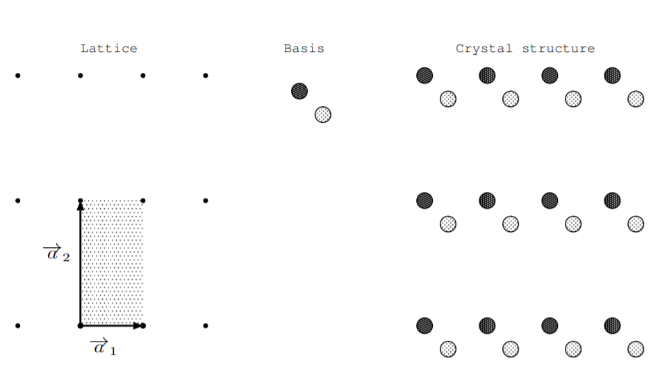
To specify the structure of a material, we attach one or more atoms to every point in the lattice. This arrangement of atoms is called a crystal basis. The lattice and crystal basis together define the crystal structure [25]. Figure \(\PageIndex{1}\) shows a two dimensional example of a lattice, crystal basis, and crystal structure. Since this example is two dimensional, only two lattice vectors are needed to specify the lattice. Two primitive lattice vectors are shown, and a primitive cell is shaded.
There are 14 possible three dimensional lattice types, and these are called Bravais lattices [25]. Each of these possible lattices has a descriptive name. Figure \(\PageIndex{2}\) shows four of the possible Bravais lattices: simple cubic, body centered cubic, face centered cubic, and asymmetric triclinic. In the simple cubic lattice, all angles between line segments connecting nearest neighbor points are right angles, and all lengths between nearest neighbor points are equal. In the asymmetric triclinic lattice, none of these angles are right angles, and none of these lengths between nearest neighbor points are equal. Figure \(\PageIndex{2}\) shows lattice cells, but the cells for the body centered cubic and face centered cubic lattices are not primitive cells because smaller repeating units can be found.
Consider some example lattices and crystal structures. The crystal structure of sodium chloride, for example, involves a face centered cubic lattice and a basis composed of one sodium and one chlorine atom. Another example is silicon which crystallizes in what is known as the diamond structure [25]. This crystal structure involves a face centered cubic lattice and a basis composed of two silicon atoms, at location (0, 0, 0) and \((\frac{l}{4},\frac{l}{4},\frac{l}{4})\)where \(l\) is the length of the primitive cell. Carbon, \(\text{Si}\), \(\text{Ge}\), and \(\text{Sn}\) all crystallize in this diamond structure with cell lengths of \(l\) = 0.356, 0.543, 0.565, and 0.646 nm respectively [25].
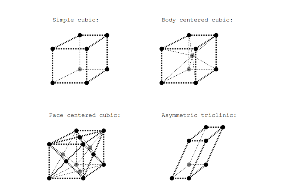
Figure \(\PageIndex{2}\): Illustration of some Bravais lattices.
While there are only 14 possible three dimensional lattices, there are significantly more possible crystal structures because the crystal structure also incorporates the basis. It is not possible to list all possible crystal structures. Instead, they are classified based on the symmetries they contain. Possible symmetry operations are 2-fold, 3-fold, 4-fold, and 6-fold rotations, horizontal and vertical mirror planes, and inversion. Crystal structures are grouped based on the symmetry elements they contain into classes called crystal point groups. There are 32 possible crystal point groups, and they are listed in the Table \(\PageIndex{1}\).
Some authors classify crystal structures into crystal space groups instead of crystal point groups [6] [26]. While there are 32 crystal point groups, there are 230 crystal space groups. Crystal space groups are based on symmetry transformations which can incorporate not only rotations and mirror planes but also combination of translations along with rotations and mirror planes. Crystal space groups will not be discussed further in this text.
| Hermann- Mauguin Notation | Schoenflies Notation | Crystal System | Angles of Primitive Lattice Cell | Lengths of Primitive Lattice Cell | Piezoelec., Pockels Electro- optic, No Inversion Symmetry | Pyroelectric |
|---|---|---|---|---|---|---|
| 1 | \(C_1\) | triclinic | \( \alpha , \beta , \gamma \neq 90^{\circ} \) | \(a \neq b \neq c\) | y | y |
| \(\bar{1}\) | \(S_2\) | triclinic | \( \alpha , \beta , \gamma \neq 90^{\circ} \) | \(a \neq b \neq c\) | n | n |
| 2 | \(C_2\) | monoclinic | \( \alpha , \gamma = 90^{\circ}, \beta \neq 90^{\circ} \) | \(a \neq b \neq c\) | y | y |
| \(m\) | \(C_{1h}\) | monoclinic | \( \alpha , \gamma = 90^{\circ}, \beta \neq 90^{\circ} \) | \(a \neq b \neq c\) | y | y |
| \(\frac{2}{m}\) | \(C_{2h}\) | monoclinic | \( \alpha , \gamma = 90^{\circ}, \beta \neq 90^{\circ} \) | \(a \neq b \neq c\) | n | n |
| 222 | \(D_2, V\) | orthorhombic | \( \alpha , \beta , \gamma = 90^{\circ} \) | \(a \neq b \neq c\) | y | n |
| 2mm | \(C_{2v}\) | orthorhombic | \( \alpha , \beta , \gamma = 90^{\circ} \) | \(a \neq b \neq c\) | y | y |
| \(\frac{2}{m}\frac{2}{m}\frac{2}{m}\) | \(D_{2h}, V_h\) | orthorhombic | \( \alpha , \beta , \gamma = 90^{\circ} \) | \(a \neq b \neq c\) | n | n |
| 4 | \(C_4\) | tetragonal | \( \alpha , \beta , \gamma = 90^{\circ} \) | \(a = b \neq c\) | y | y |
| \(\bar{4}\) | \(S_4\) | tetragonal | \( \alpha , \beta , \gamma = 90^{\circ} \) | \(a = b \neq c\) | y | n |
| \(\frac{4}{m}\) | \(C_{4h}\) | tetragonal | \( \alpha , \beta , \gamma = 90^{\circ} \) | \(a = b \neq c\) | n | n |
| 422 | \(D_4\) | tetragonal | \( \alpha , \beta , \gamma = 90^{\circ} \) | \(a = b \neq c\) | y | n |
| \(4mm\) | \(C_{4v}\) | tetragonal | \( \alpha , \beta , \gamma = 90^{\circ} \) | \(a = b \neq c\) | y | y |
| \(\bar{4}2m\) | \(D_{2d}, V_d\) | tetragonal | \( \alpha , \beta , \gamma = 90^{\circ} \) | \(a = b \neq c\) | y | n |
| \(\frac{4}{m}\frac{2}{m}\frac{2}{m}\) | \(D_{4h}\) | tetragonal | \( \alpha , \beta , \gamma = 90^{\circ} \) | \(a = b \neq c\) | n | n |
| 3 | \(C_3\) | trigonal | \( \alpha , \beta , \gamma \neq 90^{\circ} \) | \(a = b = c\) | y | y |
| \(\bar{3}\) | \(S_6\) | trigonal | \( \alpha , \beta , \gamma \neq 90^{\circ} \) | \(a = b = c\) | n | n |
| 32 | \(D_3\) | trigonal | \( \alpha , \beta , \gamma \neq 90^{\circ} \) | \(a = b = c\) | y | n |
| \(3m\) | \(C_{3v}\) | trigonal | \( \alpha , \beta , \gamma \neq 90^{\circ} \) | \(a = b = c\) | y | y |
| \(\bar{3}\frac{2}{m}\) | \(D_{3d}\) | trigonal | \( \alpha , \beta , \gamma \neq 90^{\circ} \) | \(a = b = c\) | n | n |
| 6 | \(C_6\) | hexagonal | \( \alpha = \beta = 90^{\circ}, \gamma = 120^{\circ} \) | \(a = b \neq c\) | y | y |
| \(\bar{6}\) | \(C_{3h}\) | hexagonal | \( \alpha = \beta = 90^{\circ}, \gamma = 120^{\circ} \) | \(a = b \neq c\) | y | n |
| \(\frac{6}{m}\) | \(C_{6h}\) | hexagonal | \( \alpha = \beta = 90^{\circ}, \gamma = 120^{\circ} \) | \(a = b \neq c\) | n | n |
| 622 | \(D_6\) | hexagonal | \( \alpha = \beta = 90^{\circ}, \gamma = 120^{\circ} \) | \(a = b \neq c\) | y | n |
| \(6mm\) | \(C_{6v}\) | hexagonal | \( \alpha = \beta = 90^{\circ}, \gamma = 120^{\circ} \) | \(a = b \neq c\) | y | y |
| \(\bar{6}m2\) | \(D_{3h}\) | hexagonal | \( \alpha = \beta = 90^{\circ}, \gamma = 120^{\circ} \) | \(a = b \neq c\) | y | n |
| \(\frac{6}{m}\frac{2}{m}\frac{2}{m}\) | \(D_{6h}\) | hexagonal | \( \alpha = \beta = 90^{\circ}, \gamma = 120^{\circ} \) | \(a = b \neq c\) | n | n |
| 23 | \(T\) | cubic (isometric) | \( \alpha , \beta , \gamma = 90^{\circ} \) | \(a = b = c\) | y | n |
| \(\frac{2}{3}\bar{m}\) | \(T_h\) | cubic (isometric) | \( \alpha , \beta , \gamma = 90^{\circ} \) | \(a = b = c\) | n | n |
| 432 | \(O\) | cubic (isometric) | \( \alpha , \beta , \gamma = 90^{\circ} \) | \(a = b = c\) | y | n |
| \(\bar{4}3m\) | \(T_d\) | cubic (isometric) | \( \alpha , \beta , \gamma = 90^{\circ} \) | \(a = b = c\) | y | n |
| \(\frac{4}{m}\bar{3}\frac{2}{m}\) | \(O_h\) | cubic (isometric) | \( \alpha , \beta , \gamma = 90^{\circ} \) | \(a = b = c\) | n | n |
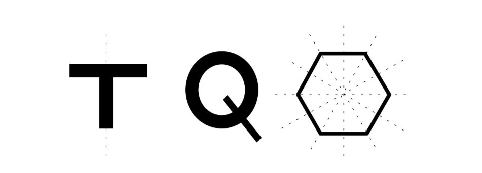
As an example of identifying symmetry elements, consider the 2D shapes in Figure \(\PageIndex{3}\). The T-shaped figure has one symmetry element, a mirror plane symmetry. The shape looks the same if it is reflected over the mirror plane shown in the figure by a dotted line. The Q-shape has no symmetry elements. The hexagon has multiple symmetry elements. It contains 2-fold rotation because it looks the same when rotated by \(180^{\circ}\). It also has 3-fold and 6-fold rotation symmetries because it looks the same when rotated by \(60^{\circ}\) and \(30^{\circ}\) respectively. It also has multiple mirror planes shown by dotted lines in the figure. In this example, symmetry elements of 2D shapes are identified, but material scientists are interested in identifying symmetries of 3D crystal structures to gain insights in the properties of materials. Materials are classified into categories called crystal point groups based on the symmetries of their crystal structures.
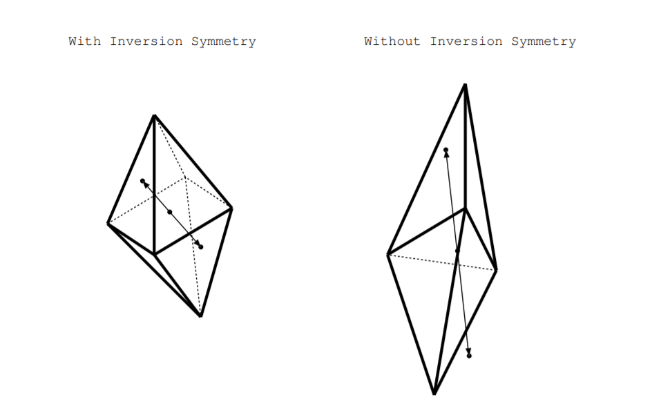
We generalize about crystalline materials based on whether or not their crystal structure possesses inversion symmetry. What is the inversion operation? In 2D, inversion is the same as a rotation by \(180^{\circ}\). In 3D, a shape or crystal structure contains inversion symmetry if it is identical when rotated by \(180^{\circ}\) and inverted through the origin [24, p. 269]. More specifically, draw a vector \(\overrightarrow{V}\) from the center of the shape to any point on the surface. If the shape has inversion symmetry, then for any such vector \(\overrightarrow{V}\), the point a distance \(\overrightarrow{V}\) from the origin is also on the surface of the shape. The example on the left of Figure \(\PageIndex{4}\) has inversion symmetry because for any such vector \(\overrightarrow{V}\) from the center of the shape to a point on the surface, there is a point on the surface a vector \(\overrightarrow{V}\) away from the origin too. The example on the right does not contain inversion symmetry as illustrated by the vector \(\overrightarrow{V}\) shown by the arrow.
If a crystal structure has inversion symmetry, we say the crystal has a center of symmetry otherwise we say it is noncentrosymmetric. Crystal structures are classified into classes called crystal point groups, and twenty-one of the 32 point groups have no center of symmetry thus do not contain inversion symmetry [24, p. 35]. Twenty of these crystal point groups have a polar axis, some axis in the crystal with different forms on opposite ends of the axis. These twenty one crystal point groups are specified as noncentrosymmetric in the sixth column of Table \(\PageIndex{1}\). If we mechanically stress these materials along the polar axis, different amounts of charges will build up on the different sides of the axis. Dielectric crystalline materials whose crystal structure belongs to any one of these 21 of these noncentrosymmetric crystal point groups are piezoelectric [24].
Table \(\PageIndex{1}\) lists all crystal point groups and summarizes whether crystalline materials whose crystal structure belongs to each group can be piezoelectric, pyroelectric, and Pockels electro-optic. Pyroelectricity and electro-optics are discussed in the next chapter. Information in the table comes from references [24] [26] [27] [28]. The left two column list the 32 possible crystal point groups. There are two different, but equivalent, ways of labeling the crystal point groups. The first column names the crystal point groups using Hermann-Mauguin notation. This notation dates to the 1930s and is used by chemists, mineralogists, and some physicists. The second column names the crystal point groups using Schoenflies notation. Schoenflies notation dates from 1891 [29], and it is used by mathematicians, spectroscopists, and other physicists.

The third column of Table \(\PageIndex{1}\) lists the crystal system. As shown in Figure \(\PageIndex{5}\):, the angles of a primitive cell of a lattice are labeled \(\alpha,\) \(\beta,\) and \(\gamma\), and the lengths of the sides are labeled \(a,\) \(b,\) and \(c\). Crystal point groups can be classified based on the angles and lengths of the primitive cell of the lattice which belongs to that group. The literature contains multiple subtly different ways of defining crystal systems [30]. The information in the third column follows reference [28]. The fourth column gives relationships between the angles of the primitive cell. The fifth column gives relationships between the lengths of sides of the primitive cell. Combinations of angles and lengths are not unique to a specific row. For example, classes \(C_2\) and \(C_{1h}\) both have \(\alpha = 90^{\circ} ,\) \(\beta \neq 90^{\circ} ,\) \(\gamma = 90^{\circ}\), and \(a \neq b \neq c\). However, crystal structures belonging to these crystal point groups contain different symmetry elements. For more details on specifically which symmetry elements are contained in which crystal point group, see [24] [26] [27] [28]. The sixth column lists whether or not the crystal point group has inversion symmetry. Crystal structures with no inversion symmetry or center of symmetry, called noncentrosymmetric, are both piezoelectric and Pockels electro-optic. The last column lists whether or not crystalline materials whose crystal structure belongs to the various crystal point groups can be pyroelectric.
It is possible to start with a crystal structure of a material, derive the symmetry elements it contains, derive whether or not the material is piezoelectric, and derive whether or not the material is pyroelectric. Furthermore, it is possible to derive along which axes piezoelectricity or pyroelectricity can occur in the material. However, this derivation is beyond the scope of this book. For further details, see [6] [27] [28] [31].
To predict whether or not a dielectric crystalline material is piezoelectric, identify its lattice and crystal basis to identify its crystal structure. Identify the symmetries of the crystal structure to classify its crystal structure into a particular crystal point group. If that crystal structure contains inversion symmetry, the material can be piezoelectric. We often do not have to go through all of these steps because the crystal point group for many crystalline materials is tabulated [32]. Even if the crystal structure for a material contains inversion symmetry, the piezoelectric effect and the piezoelectric strain coeficient \(d\) may be too small to measure.
The effect may only occur when you stress the material along some particular axis, and it may not occur for a mechanical stress of an arbitrary orientation with respect to the direction of the crystal axes. There is only one crystal point group, called asymmetric triclinic, where a random stress will produce a material polarization [24]. For all other point groups, only stresses along certain axes will produce a material polarization [24]. Furthermore, in most crystals a given amount of stress along one axis of the crystal will produce a different amount of material polarization than the same amount of stress applied along a different crystallographic axis. Qualitatively, compressing a crystal along one axis may cause more charge displacement than compressing a crystal along a different axis. For this reason, it is more accurate to treat the piezoelectric strain coeficient as a matrix. This 3x6 matrix has elements \[d_{ik} =\left. \left(\frac{\partial\text{strain along k}}{\partial\text{electric field along i}}\right)\right|_{\text{for a given stress}} \nonumber \]
where electric field has \(x,\) \(y,\) and \(z\) components, and the stress can be applied along the \(xx,\) \(xy,\) \(xz,\) \(yy,\) \(yz,\) or \(zz\) directions.
Piezoelectricity in Amorphous and Polycrystalline Materials and Ferroelectricity
The previous section discussed piezoelectricity in crystals. We can discuss symmetries of the crystal structure of crystalline materials, but we cannot even define a crystal structure for amorphous materials. However, it is possible to make piezoelectric devices out of polycrystalline and amorphous materials. In a dielectrics, if we apply an external electric field, a material polarization is induced. Electric dipoles form because the electrons and nuclei of the atoms displace slightly from each other. Coulomb's law tells us that charge buildups, such as these electric dipoles, induce an electric field. So, if we apply an external electric field to a dielectric, this primary effect induces a material polarization, and this material polarization will, as a secondary effect, induce additional material polarization in the material. Once one atom polarizes forming an electric dipole, nearby atoms will polarize. Small regions of the same material polarization are called electrical domains.
In certain dielectric materials, an external mechanical stress induces a local material polarization. The charge buildup of this material polarization induces a material polarization in nearby atoms forming electrical domains [23]. This piezoelectric effect can occur whether the original material is crystalline, amorphous, or polycrystalline [23]. In noncrystalline materials, this effect is necessarily nonlinear, so these materials are not well described by Equations \ref{2.3.1} or \ref{2.3.6}.
The nonlinear process of a material polarization of one atom inducing a material polarization of nearby atoms causing the formation of electrical domains is called ferroelectricity. Ferroelectric materials may be crystalline, amorphous, or polycrystalline. We will see in the next chapter that materials can be ferroelectric pyroelectric and ferroelectric electro-optic in addition to ferroelectric piezoelectric. The ferroelectric effect is limited by temperature. For many ferroelectric materials, these effects occur only below some temperature, called the Curie temperature. When the materials are heated above the Curie temperature, the ferroelectric effect goes away [33]. The material polarization of a ferroelectric material may depend on whether or not a material polarization has previously been induced. If the state of a material depends on its past history, we say that the material has hysteresis. Ferroelectric materials may have a material polarization even in the absence of an external mechanical stress or electric field if a source of energy has previously been applied.
While the prefix ferro- means iron, most ferroelectric materials do not contain iron, and most iron containing materials are not ferroelectric. The word ferroelectric is used as an analogy to the word ferromagnetic. Some iron containing materials are ferromagnetic. If an external magnetic field is applied across a ferromagnetic material, an internal magnetic field is set up in the material. Ferromagnetic materials can have a permanent magnetic dipole even in the absence of an applied magnetic field. We can model an electric dipole as a pair of charges. We can model a magnetic dipole as a small current loop. Ferromagnetic materials exhibit hysteresis, and they have magnetic domains where the magnetic dipoles are aligned.
Originally, a piezoelectric ferroelectric material has randomly aligned electrical domains and no net material polarization, so it starts out as neither piezoelectric or ferroelectric. The process of causing a material to exhibit piezoelectricity and ferroelectricity is called poling. To pole a material, place it in a strong external electric field [23], for example, across the poles of a battery, hence the term. Poling does not change the atomic structure, so if the material was originally amorphous, it will remain amorphous. During this process, electrical domains form, and these domains remain even when the external field is removed. A material that is piezoelectric due to this type of poling is sometimes called an electret [15, p. 297]. After the material is poled, it may have a net material polarization throughout. Furthermore after poling, it is piezoelectric and ferroelectric, so an external mechanical stress induces a material polarization locally and throughout the material.
Materials Used to Make Piezoelectric Devices
What makes a good material for a piezoelectric sensor or piezoelectric energy conversion device? First piezoelectric devices are made from electrical insulators. When an external voltage is applied across a conductor, valence electrons are removed from their atoms, so no material polarization accumulates. Second, piezoelectric devices are made from materials with large piezoelectric strain constants. The piezoelectric strain constant is so small that it cannot be detected in many crystals with crystal structures from one of the 21 crystal point groups known to be piezoelectric, and it is zero in crystals from the other crystal point groups. Third, piezoelectric devices should be made from materials that are not brittle so that they can withstand repeated stressing without permanent damage. Thermal properties may also be important [33]. There is no material that is best in all applications.
Quartz, crystalline \(\text{SiO}_2\), was the first material in which piezoelectricity was studied. Pierre and Jacques Curie discovered the effect in quartz in the 1880s [3]. Today, many piezoelectric devices, including crystal oscillators, are made from quartz. Lead zirconium titanate is another material used due to its relatively high piezoelectric strain constant [3] [34]. In applications which require flexibility and the ability to withstand repeated mechanical stress without damage, polymers such as polyvinyldenfluoride are used [25]. Piezoelectricity has also been studied in materials including barium titanate \(\text{BaTiO}_3\), lithium niobate, tourmaline
\[\text{(Na,Ca)(Li,Mg,Al)}_3 \text{(Al,Fe,Mn)}_6 ( \text{BO}_3)_3 (\text{Si}_6\text{O}_8)\text{(OH)}_4 , \nonumber \]
and Rochelle salt
\[\text{KNaC}_4\text{H}_4\text{O}_6 \cdot 4\text{H}_2\text{O} \nonumber \]
[3] [23] [24] [34].
Manufacturers of piezoelectric devices do not often label their products to say whether they are made from crystalline, amorphous, or polycrystalline materials, but there are advantages and disadvantages to the different types of materials. An advantage of making piezoelectric devices from polycrystalline or amorphous materials is that the devices can be made more easily into different shapes such as cylinders and spheres [33]. However, the materials used often have lower melting temperatures, higher temperature expansion coeficients, and are more brittle [33]. Crystalline materials, such as quartz, have the advantages of being harder and having a higher melting temperature [33].
Applications of Piezoelectricity
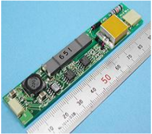
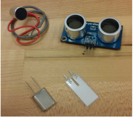
A number of electrical components involve piezoelectricity. When a voltage is applied across a piece of piezoelectric material, it mechanically bends and deforms. When the voltage is released, it springs back at a natural resonant frequency. This material can be integrated with a feedback circuit to produce oscillations at a precise frequency. Electrical oscillators of this type are often made from crystalline quartz. A more recent application is the piezoelectric transformer. These devices are used in the cold cathode fluorescent lamps which are used as backlight for LCD panels [23, p. 289]. The lamps require around a thousand volts to turn on and hundreds of volts during use. Transformers made of magnets and coils can achieve these high voltages, but piezoelectric transformers are much smaller, small enough to be mounted on a printed circuit board. A traditional transformer involves a pair of coils, and it converts AC electricity to magnetic energy to AC electricity at a different voltage. Similarly, a piezoelectric transformer also involves multiple energy conversion processes. In such a device, AC electricity is converted to mechanical vibrations and then to AC electricity at a different voltage. Energy is conserved in these devices, so they can produce high voltages with low currents. Figure \(\PageIndex{6}\): shows a piezoelectric transformer that can convert an input of 8 to 14 V to an output up to 2 kV [35]. Figure \(\PageIndex{7}\): shows an example of some small piezoelectric circuit components. Starting in the upper left and going clockwise, a microphone, ultrasonic transmitter and receiver, vibration sensor, and oscillator are shown.
Efficiency of energy conversion devices is hard to discuss because every author makes different assumptions. However by any measure, efficiency of a commercial piezoelectric device is low, often 6% or less [36]. Due to this low efficiency, many piezoelectric devices are used as sensors. Regardless of this low efficiency, other devices are used for energy harvesting. For example, one train station embedded piezoelectric devices in the platforms to generate electricity. Piezoelectric devices also have been used to convert the energy from the motion of a fluid or from wind directly to electricity [36].
There is interest in using piezoelectric devices for biomedical applications. Quartz is piezoelectric, and it is durable, readily available, and nontoxic. Engineers have developed piezoelectric devices designed for use outside of the body and to be implanted inside the body. Some piezoelectric devices are used as sensors. For example, piezoelectric sensors can monitor knees or other joints [3]. Also, ultrasonic imaging is a common diagnostic technique. Piezoelectric devices are used both to generate the ultrasonic vibrations and to detect them [33]. Other biomedical piezoelectric devices are used as a source of electrical power. Artificial hearts, pacemakers, and other devices require electricity, and they are often limited by battery technology available to supply the energy [36]. Piezoelectric generators have no moving parts to wear out, and they can avoid the problem of needing to change the batteries. Physical activity can be classified as continuous, such as breathing, or discontinuous, such as walking. Both types of physical activity can be used as a source of mechanical energy for piezoelectric devices [36]. The amount of power required for different biomedical devices varies quite a bit. For example, an artificial heart may require around 8 W while a pacemaker may require only a few microwatts [36]. Piezoelectric devices may be able to capture energy from typical physical activity and convert it into electrical energy to power the device. A piezoelectric device in an artificial knee has produced 0.85 mW [36], and a device in a shoe has generated 8.4 mW from walking [36].
Piezoelectric devices are used in other types of imaging systems besides biomedical imaging systems. One of the earlier applications was in sonar systems. Around the time of WWI, the military actively developed sonar systems to detect boats and submarines. Today, sonar systems are used to detect fish and to measure the depth of bodies of water [33]. Sonar imaging is also used to analyze electrical circuits and to detect imperfections and cracks in steel and in welds [33].
Piezoelectric devices are used in a variety of other applications too. Piezoelectric sensors are used in some buttons and keyboards [36]. Piezoelectric devices are used to make accelerometers [37, p. 353], and they are used to measure pipe flow [33]. Speakers, microphones and buzzers can all be made from piezoelectric devices, and they can operate at both audio and ultrasonic frequencies. Piezoelectric devices that generate ultrasonic signals can be used to emulsify dyes, paints, and food products like peanut butter [33]. Also, they are used in some barbecue grill ignitions where mechanical stress induces an electric spark [23, ch. 15].