Engineering LibreTexts

5.2: FET switching

  • Page ID
    51319
  • \( \newcommand{\vecs}[1]{\overset { \scriptstyle \rightharpoonup} {\mathbf{#1}} } \) \( \newcommand{\vecd}[1]{\overset{-\!-\!\rightharpoonup}{\vphantom{a}\smash {#1}}} \)\(\newcommand{\id}{\mathrm{id}}\) \( \newcommand{\Span}{\mathrm{span}}\) \( \newcommand{\kernel}{\mathrm{null}\,}\) \( \newcommand{\range}{\mathrm{range}\,}\) \( \newcommand{\RealPart}{\mathrm{Re}}\) \( \newcommand{\ImaginaryPart}{\mathrm{Im}}\) \( \newcommand{\Argument}{\mathrm{Arg}}\) \( \newcommand{\norm}[1]{\| #1 \|}\) \( \newcommand{\inner}[2]{\langle #1, #2 \rangle}\) \( \newcommand{\Span}{\mathrm{span}}\) \(\newcommand{\id}{\mathrm{id}}\) \( \newcommand{\Span}{\mathrm{span}}\) \( \newcommand{\kernel}{\mathrm{null}\,}\) \( \newcommand{\range}{\mathrm{range}\,}\) \( \newcommand{\RealPart}{\mathrm{Re}}\) \( \newcommand{\ImaginaryPart}{\mathrm{Im}}\) \( \newcommand{\Argument}{\mathrm{Arg}}\) \( \newcommand{\norm}[1]{\| #1 \|}\) \( \newcommand{\inner}[2]{\langle #1, #2 \rangle}\) \( \newcommand{\Span}{\mathrm{span}}\)\(\newcommand{\AA}{\unicode[.8,0]{x212B}}\)

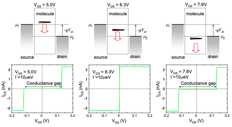
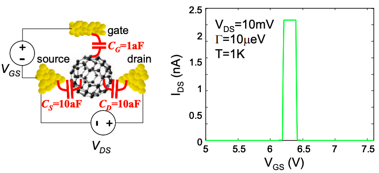
    In digital circuits, an ideal FET has two states, ON and OFF, selected by the potential applied to the gate. In the OFF state, the channel is closed to the flow of electrons even if a bias is applied between the source and drain electrodes. To close the channel, the gate must prevent the injection of electrons from the source. For example, consider the molecular FET in Figure 5.2.1. Here, we follow FET convention and measure all potentials relative to a grounded source contact. For a gate bias of \(V_{GS}< \sim 6.2V\) little current flows through the molecule. But for \(\sim 6.2V < V_{GS}< \sim 6.4V\) the FET is ON and the channel is conductive.

    Screenshot 2021-05-12 at 22.26.03.png
    Figure \(\PageIndex{1}\): The \(I_{DS} - V_{GS}\) characteristics of a FET employing the buckyball molecule C60. At equilibrium the source and drain chemical potentials are at -5eV, and the molecule's LUMO is at -4.7eV. The various electrostatic capacitances in the device are labeled. As the gate potential is increased, the LUMO is pushed lower. At approximately \(V_{GS} = 6.3 V\), it is pushed into resonance with the source and drain contacts and the current increases dramatically. The width of the LUMO determines the sharpness of the resonance. Note 'aF' is the symbol for atto Farad (\(10^{-18} F\)).

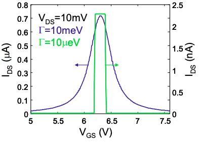
    As shown in Figure 5.2.2, the transitions are much more gradual if the molecular energy level is broader. Similarly, increasing the temperature can also blur the switching characteristics.

    Screenshot 2021-05-12 at 22.32.00.png
    Figure \(\PageIndex{2}\): A comparison between the switching characteristics of molecular FETs with broad and narrow energy levels. Note the different current scales.

    The origin of FET switching is explained in Figure 5.2.3. The gate potential acts to shift energy levels in the molecule relative to the contact chemical potentials. When an energy level is pushed between \(\mu_{1}\) and \(\mu_{2}\) electrons can be injected from the source. Correspondingly, the current is observed to increase. Further increases in gate potential push the energy level out of resonance and the current decreases again at ~6.4V.

    Screenshot 2021-05-12 at 22.34.10.png
    Figure 5.2.1. Outside resonance a conductance gap opens because additional source-drain bias is required to pull the molecular level between the source and drain chemical potentials.

    This page titled 5.2: FET switching is shared under a CC BY-NC-SA 4.0 license and was authored, remixed, and/or curated by Marc Baldo (MIT OpenCourseWare) via source content that was edited to the style and standards of the LibreTexts platform; a detailed edit history is available upon request.