Engineering LibreTexts

5.3: FET Calculations

  • Page ID
    51320
  • \( \newcommand{\vecs}[1]{\overset { \scriptstyle \rightharpoonup} {\mathbf{#1}} } \) \( \newcommand{\vecd}[1]{\overset{-\!-\!\rightharpoonup}{\vphantom{a}\smash {#1}}} \)\(\newcommand{\id}{\mathrm{id}}\) \( \newcommand{\Span}{\mathrm{span}}\) \( \newcommand{\kernel}{\mathrm{null}\,}\) \( \newcommand{\range}{\mathrm{range}\,}\) \( \newcommand{\RealPart}{\mathrm{Re}}\) \( \newcommand{\ImaginaryPart}{\mathrm{Im}}\) \( \newcommand{\Argument}{\mathrm{Arg}}\) \( \newcommand{\norm}[1]{\| #1 \|}\) \( \newcommand{\inner}[2]{\langle #1, #2 \rangle}\) \( \newcommand{\Span}{\mathrm{span}}\) \(\newcommand{\id}{\mathrm{id}}\) \( \newcommand{\Span}{\mathrm{span}}\) \( \newcommand{\kernel}{\mathrm{null}\,}\) \( \newcommand{\range}{\mathrm{range}\,}\) \( \newcommand{\RealPart}{\mathrm{Re}}\) \( \newcommand{\ImaginaryPart}{\mathrm{Im}}\) \( \newcommand{\Argument}{\mathrm{Arg}}\) \( \newcommand{\norm}[1]{\| #1 \|}\) \( \newcommand{\inner}[2]{\langle #1, #2 \rangle}\) \( \newcommand{\Span}{\mathrm{span}}\)\(\newcommand{\AA}{\unicode[.8,0]{x212B}}\)

    Unlike the two terminal case, where we arbitrarily set \(E_{F} = 0\) and shifted the Source and Drain potentials under bias, the FET convention fixes the Source electrode at ground. There are two voltage sources: \(V_{GS}\), the gate potential, and \(V_{DS}\), the drain potential. We analyze the influence of \(V_{GS}\) and \(V_{DS}\) on the molecular potential using capacitive dividers and superposition:

    Screenshot 2021-05-12 at 22.37.14.png
    Figure \(\PageIndex{1}\): Analyzing a molecular FET using a capacitive divider and superposition.

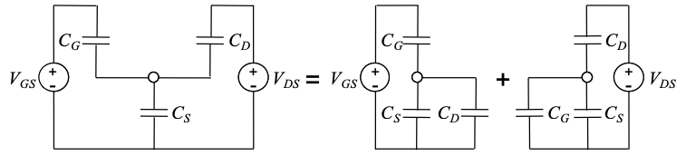
    \[ U_{E S}=-q V_{G S} \frac{1 /\left(C_{D}+C_{S}\right)}{1 /\left(C_{D}+C_{S}\right)+1 / C_{G}}-q V_{D S} \frac{1 /\left(C_{G}+C_{S}\right)}{1 /\left(C_{G}+C_{S}\right)+1 / C_{D}} \nonumber \]

    Simplifying, and noting that the total capacitance at the molecule is \(C_{ES} = C_{S} + C_{D} + C_{G}\):

    \[ U_{ES} = -qV_{GS}\frac{C_{G}}{C_{ES}}-qV_{DS} \frac{C_{D}}{C_{ES}} \nonumber \]

    We also must consider charging. As before,

    \[ U_{C} = -\frac{q^{2}}{C_{ES}}(N-N_{0}) \nonumber \]

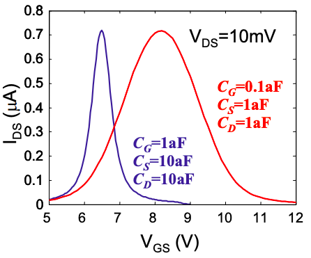
    Recall that charging opposes shifts in the potential due to \(V_{GS}\) or \(V_{DS}\). Thus, if charging is significant, the switching voltage increases; see Figure 5.3.2.

    Screenshot 2021-05-12 at 22.43.20.png
    Figure 5.2.1 calculated under two different sets of capacitances. Charging is more important for the smaller capacitances. The switching voltage for this device is observed to increase to ~8.1V.

    Adding the static potential due to \(V_{DS}\) and \(V_{GS}\) gives, the potential U in terms of the charge, N, and bias.

    \[ U=-qV_{GS} \frac{C_{G}}{C_{ES}}-qV_{DS}\frac{C_{D}}{C_{ES}}+\frac{q^{2}}{C_{ES}}(N-N_{0}) \nonumber \]

    We also have an expression for potential for N in terms of U (see Equation (3.7.8))

    \[ N = \int^{\infty}_{-\infty} g(E-U) \frac{\tau_{D}f(E,\mu_{S})+\tau_{S}f(E, \mu_{D})}{\tau_{S}+\tau_{D}} dE \nonumber \]

    As before, Equations (5.3.4) and (5.3.5) must typically be solved iteratively to obtain U. Then we can solve for the current using:

    \[ I = q\int^{\infty}_{-\infty} g(E-U)\frac{1}{\tau_{S}+\tau_{D}} \left(f(E,\mu_{S})-f(E,\mu_{D})\right)dE \nonumber \]


    This page titled 5.3: FET Calculations is shared under a CC BY-NC-SA 4.0 license and was authored, remixed, and/or curated by Marc Baldo (MIT OpenCourseWare) via source content that was edited to the style and standards of the LibreTexts platform; a detailed edit history is available upon request.