
5.8: Cascaded Lines
- Page ID
- 88572

We can use bounce diagrams to handle somewhat more complicated problems as well.
Arnold Aggie decides to add an additional ethernet interface to the one already connected to his computer. He decides just to add a "T" to the terminal where the cable is connected to his "thin-net" interface, and add on some more wire. Unfortunately, he is not careful about the coaxial cable he uses, and so he has some \(75 \mathrm{~ \Omega}\) TV co-ax instead of the \(50 \mathrm{~ \Omega}\) ethernet cable. He ends up with the situation shown in Figure \(\PageIndex{1}\). This kind of problem is called a cascaded line problem because we have two different lines, one hooked up after the other. The analysis is similar to what we have done before, just a little more complicated is all.
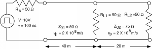 Figure \(\PageIndex{1}\): Cascaded line problem
We will have to do a little more thinking before we can draw out the bounce diagram for this problem. The driver for ethernet cable coming to Arnold's computer can be modeled as a \(10 \mathrm{~V}\) (open circuit) source with a \(50 \mathrm{~\Omega}\) internal impedance. Since the source does not (initially) know anything about how the line it is driving is terminated, the first signal \(V_{1}^{+}\) will be the same as in our initial problem, in this case just a +\(5 \mathrm{~V}\) signal headed down the line.
Let's focus on the "T" for a minute, as shown in Figure \(\PageIndex{2}\).
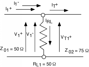 Figure \(\PageIndex{2}\): At the junction
\(V_{1}^{+}\) is incident on the junction. When it hits the junction, there will be a reflected wave \(V_{1}^{-}\) and also now a transmitted wave \(V_{T1}^{+}\). Since the incident wave can not tell the difference between a \(75 \mathrm{~\Omega}\) resistor and a \(75 \mathrm{~\Omega}\) transmission line, it thinks it is seeing a termination resistor equal to a \(50 \mathrm{~\Omega}\) resistor (\(R_{L1}\)) in parallel with a \(75 \mathrm{~\Omega}\) resistor (the second line). \(50 \mathrm{~\Omega}\) in parallel with \(75 \mathrm{~\Omega}\) is \(30 \mathrm{~\Omega}\). Let's call this "apparent" load resistor \(R'_{L}\), so that we can then calculate \(\Gamma_{V_{12}}\), the first voltage reflection coefficient in going from line 1 to line 2 as: \[\begin{array}{l} \Gamma_{V_{12}} &=& \dfrac{R'_{L} - Z_{01}}{R'_{L} + Z_{01}} \\[4pt] &=& \dfrac{30 - 50}{30 + 50} \\ &=& -0.25 \end{array}\]
Note that we could have started from scratch and written down KVLs and KCLs for the junction \[V_{1}^{+} + V_{1}^{-} = V_{T1}^{+}\]
and \[I_{1}^{+} + I_{1}^{-} = I_{RL} + I_{T1}^{+}\]
Then, by re-writing Equation \(\PageIndex{3}\) in terms of voltage and impedances we have: \[\frac{V_{1}^{+}}{Z_{01}} - \frac{V_{1}^{-}}{Z_{01}} = \frac{V_{T1}^{+}}{Z_{02}} + \frac{V_{T1}^{+}}{R_{L}}\]
We now have two equations with two unknowns (\(V_{1}^{+}\) and \(V_{T1}^{+}\)). By solving Equation \(\PageIndex{4}\) for \(V_{T1}^{+}\) and then plugging that into Equation \(\PageIndex{2}\), we could get the ratio of \(V_{1}^{-}\) to \(V_{1}^{+}\), or the voltage reflection coefficient. The interested reader can confirm that indeed, you get the very same result this way.
In order to completely solve this problem, we also need to know \(V_{T1}^{+}\), the transmitted wave as well. Since Equation \(\PageIndex{2}\) says \(V_{T1}^{+}\) is just the sum of the incident and reflected waves on the first line \[V_{T1}^{+} = V_{1}^{+} + \Gamma_{V_{12}} V_{1}^{+}\]
We can thus write \[\frac{V_{T1}^{+}}{V_{L}^{+}} = 1 + \Gamma_{V_{12}} = \frac{R'_{L} + Z_{01}}{R'_{L} + Z_{01}} + \frac{R'_{L} - Z_{01}}{R'_{L} + Z_{01}} = \frac{2 R'_{L}}{R'_{L} + Z_{01}} = \frac{60}{30 + 50} = 0.75 \equiv T_{V_{12}}\]
An important thing to note is that \[T_{V} = 1 + \Gamma_{V}\] NOT \[T_{V} + \Gamma_{V} = 1\]
We do not "conserve" voltage at a termination, in the sense that the reflected and transmitted voltage have to add up to be the incident voltage. Rather, the transmitted voltage is the sum of the incident voltage and the reflected voltage, so that we can obey Kirchoff's voltage law.
We can now start to make our bounce diagram. We propagate a \(+5 \mathrm{~V}\) wave and a \(-5 \mathrm{~V}\) wave (separated by \(100 \mathrm{~ns}\)) down towards the junction. Since the line is \(40 \mathrm{~m}\) long, and the waves move at \(2 \times 10^{8} \ \frac{\mathrm{m}}{\mathrm{s}}\), it takes \(200 \mathrm{~ns}\) for them to get to the junction. There, a \(-1.25 \mathrm{~V}\) wave is reflected back towards the source, and a \(+3.75 \mathrm{~V}\) wave is transmitted into the second transmission line in Figure \(\PageIndex{3}\).
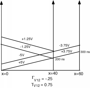
Figure \(\PageIndex{3}\): Reflection and Transmission At the "T"
Since the load for the second line is \(50 \mathrm{~\Omega}\), and the characteristic impedance, \(Z_{02}\), for the second line is \(75 \mathrm{~\Omega}\), we will have a reflection coefficient, \[\begin{array}{l} \Gamma_{V_{2}} &=& \dfrac{R_{L2} - Z_{02}}{R_{L2} + Z_{02}} \\[4pt] &=& \dfrac{50 - 75}{50 + 75} \\ &=& -0.2 \end{array}\]
Thus a \(-0.75 \mathrm{~V}\) signal is reflected off of the second load in Figure \(\PageIndex{4}\).
What is the magnitude of the voltage which is developed across the second load?
- Answer
-
3 Volts!
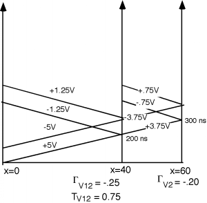 Figure \(\PageIndex{4}\): Reflection of transmitted pulse
What happens to the \(0.75 \mathrm{~V}\) pulse when it gets to the "T"? Well, there is another mismatch here, with a reflection coefficient \(\Gamma_{V_{21}}\) given by \[\begin{array}{l} \Gamma_{V_{21}} &=& \dfrac{25 - 75}{25 + 75} \\ &=& -0.5 \end{array}\]
(The \(50 \mathrm{~V}\) resistor and the \(50 \mathrm{~V}\) transmission line look like a \(25 \mathrm{~\Omega}\) termination to the \(75 \mathrm{~\Omega}\)line) and a transmission coefficient \[\begin{array}{l} T_{V_{21}} &=& 1 + \Gamma_{V_{21}} \\ &=& 0.5 \end{array}\]
and so we add to the bounce diagram in Figure \(\PageIndex{5}\).
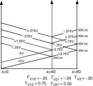 Figure \(\PageIndex{5}\): When the reflected load pulse hits the junction
We could keep going, but the voltage reflected off of the second load will only be \(75 \mathrm{~mV}\) now, so let's call it a day.
There are a couple of other interesting applications of bounce diagrams and the transient behavior of transmission lines that we might look at before we move on to other things. The first is called the Charged Line Problem. Here it is:
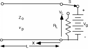 Figure \(\PageIndex{6}\): The "Charged Line" problem
We have a transmission line with characteristic impedance \(Z_{0}\) and phase velocity \(v_{p}\). It is \(L\) long, and for some time has been connected to a battery of potential \(V_{g}\) as shown in Figure \(\PageIndex{7}\). At time \(t=0\), the switch \(S\) is thrown, which removes the battery from the circuit, and connects the line to a load resistor \(R_{L}\). The question is: what does the voltage across the load resistor, \(V_{L}\), look like as a function of time? This is almost like what we have done before, but not quite.
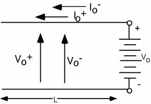 Figure \(\PageIndex{7}\): Initial conditions
In the first place, we now have non-zero initial conditions. For \(t=0\) we will have both voltages and current on the line. In order to match boundary conditions, we must do more than have one voltage and one current, because the voltage on the line must be \(V_{g}\), while the current flowing down the line must be \(0\). So, we will put in both a \(V^{+}\) and a \(V^{-}\) and their corresponding currents. Note that \(x\) is going to the left this time. Let's forget about the switch and the load resistor for a minute and just look at the line and battery. We have two equations we must satisfy: \[V_{0}^{+} + V_{0}^{-} = V_{g}\] and \[I_{0}^{+} + I_{0}^{-} = 0\]
We can use the impedance relationship to change Equation \(\PageIndex{13}\) to: \[\frac{V_{0}^{+}}{Z_{0}} - \frac{V_{0}^{-}}{Z_{0}} = 0\]
I hope most of you can then see by inspection that we must have \[\begin{array}{l} V_{0}^{+} &=& V_{0}^{-} \\[4pt] &=& \dfrac{V_{g}}{2} \end{array}\]
OK, the switch \(S\) is thrown at \(t=0\). Now the end of the line looks like Figure \(\PageIndex{8}\).
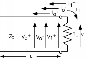
Figure \(\PageIndex{8}\): After the Resistor is Connected
We have anticipated the fact that we are going to need another voltage and current wave if we are going to be able to match boundary conditions when the load resistor is connected, and have added a \(V_{1}^{+}\) and a \(V_{1}^{-}\) to the line. These are new voltage and current waves which originate at the load resistor position in order to satisfy the new boundary conditions there. Now we do KVL and KCL again. \[V_{0}^{+} + V_{0}^{-} + V_{1}^{+} = V_{L}\] and \[\frac{V_{0}^{+}}{Z_{0}} - \frac{V_{0}^{-}}{Z_{0}} + \frac{V_{1}^{+}}{Z_{0}} = - \frac{V_{L}}{R_{L}}\]
We have already made the impedance substitution for the current equation in Equation \(\PageIndex{17}\). We know what the sum and difference of \(V_{0}^{+}\) and \(V_{0}^{-}\) are, so let's substitute these in. \[V_{g} + V_{1}^{+} = V_{L}\] and \[\frac{V_{1}^{+}}{Z_{0}} = - \frac{V_{L}}{R_{L}}\]
From this we get \[V_{L} = -\left( \frac{R_{L}}{Z_{0}} V_{1}^{+}\right)\]
which we substitute back into Equation \(\PageIndex{18}\): \[V_{g} + V_{1}^{+} = -\left( \frac{R_{L}}{Z_{0}} V_{1}^{+}\right)\]
We can then solve for \(V_{1}^{+}\): \[\begin{array}{l} V_{1}^{+} &=& -\dfrac{V_{g}}{1 + \frac{R_{L}}{Z_{0}}} \\[4pt] &=& -\left( \dfrac{Z_{0}}{R_{L} + Z_{0}} V_{g}\right) \end{array}\]
The voltage on the load is given by Equation \(\PageIndex{18}\) and is clearly just: \[V_{L} = V_{g} - \frac{Z_{0}}{R_{L} + Z_{0}} V_{g}\]
and in particular, when \(R_{L}\) is chosen to be \(Z_{0}\) (which is usually done when this circuit is used), we have \[V_{L} = \frac{V_{g}}{2}\]
Now what do we do? We build a bounce diagram! Let us stay with the assumption that \(R_{L} = Z_{0}\), in which case the reflection coefficient at the resistor end is \(0\). At the open circuit end of the transmission line \(\Gamma\) is \(+1\). So we have Figure \(\PageIndex{9}\).
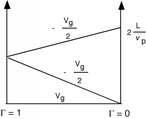 Figure \(\PageIndex{9}\): Bounce diagram for the charged line problem
Note that for this bounce diagram, we have added an additional voltage, \(V_{g}\), on the baseline to indicate that there is an initial voltage on the line, before the switch is thrown, and \(t\) starts on the bounce diagram.
If we concentrate on the voltage across the load, we add \(V_{g}\) and \(-\frac{V_{g}}{2}\) and find that the voltage across the load resistor rises to \(\frac{V_{g}}{2}\) at time \(t=0\) in Figure \(\PageIndex{10}\). The \(-\frac{V_{g}}{2}\) voltage wave travels down the line, hits the open circuit, reflects back, and when it gets to the load resistor, brings the voltage across the load resistor back down to zero. We have made a pulse generator!
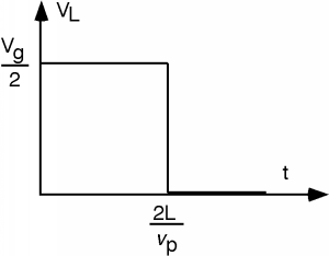 Figure \(\PageIndex{10}\): Voltage \(V_{L}\) across the load resistor \(R_{L}\)
In today's digital age, this might seem like a strange way to go about creating a pulse. Imagine, however, if you needed a pulse with a very large potential (hundreds of thousands or even millions of volts) for, say, a particle accelerator. It is unlikely that a MOSFET will ever be built which is up to the task! In fact, in a field of study called pulsed power electronics just such circuits are used all the time. Sometimes they are built with real transmission lines, sometimes they are built from discrete inductors and capacitors, hooked together just as in the distributed parameter model. Such circuits are called pulse forming networks or PFNs for short.
Finally, just because it affords us a good opportunity to review how we got to where we are right now, let's consider the problem of a non-resistive load on the end of a line. Suppose the line is terminated with a capacitor! For simplicity, let's let\(R_{s} = Z_{0}\), so when switch \(S\) is closed a wave \(V_{1}^{+} = \frac{V_{g}}{2}\) heads down the line as in Figure \(\PageIndex{11}\). Let's think about what happens when it hits the capacitor. We know we need to generate a reflected signal \(V_{1}^{-}\), so let's go ahead and put this in Figure \(\PageIndex{12}\), along with its companion current wave.
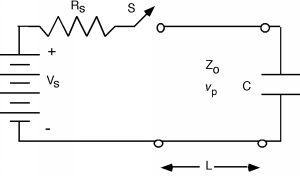 Figure \(\PageIndex{11}\): Transient problem with capacitive load
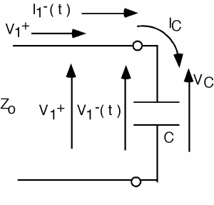 Figure \(\PageIndex{12}\): Initial pulse hits the load
The capacitor is initially uncharged, and we know we can not instantaneously change the voltage across a capacitor (at least without an infinite current!) and so the initial voltage across the capacitor should be zero, making \(V_{1}^{-} (0) = -V_{1}^{+}\), if we make time \(t=0\) be when the initial wave just gets to the capacitor. So, at \(t=0\), \(\Gamma_{V}(0) = -1\). Note that we are making \(\Gamma\) a function of time now, as it will change depending upon the charge state of the capacitor.
The current into the capacitor, \(I_{C}\), is just \(I_{1}^{+} - I_{1}^{-}(t)\). \[\begin{array}{l} I_{C}(0) &=& I_{1}^{+} + I_{1}^{-}(0) \\[4pt] &=& \dfrac{V_{g}}{Z_{0}} \end{array}\] since \[\begin{array}{l} I_{1}^{+} &=& \dfrac{V_{1}^{+}}{Z_{0}} \\[4pt] &=& \dfrac{V_{g}}{2 Z_{0}} \end{array}\] and \[\begin{array}{l} I_{1}^{-} (0) &=& -\dfrac{V_{1}}{Z_{0}} \\[4pt] &=& \dfrac{V_{g}}{2 Z_{0}} \end{array}\]
How will the current into the capacitor, \(I_{C}(t)\), behave? We have to remember the capacitor equation: \[\begin{array}{l} I_{C} (t) &=& C \dfrac{\text{d} V_{C}(t)}{\text{d} t} \\[4pt] &=& C \left(\dfrac{\partial \left(V_{1}^{+} + V_{1}^{-}(t)\right)}{\partial t}\right) \\[4pt] &=& C \dfrac{\text{d} V_{1}^{-}(t)}{\text{d} t} \end{array}\] since \(V_{1}^{+}\) is a constant and hence has a zero time derivative. Well, we also know that \[\begin{array}{l} I_{C}(t) &=& I_{1}^{+} + I_{1}^{-}(t) \\[4pt] &=& \dfrac{V_{1}^{+}}{Z_{0}} - \dfrac{V_{1}^{-} (t)}{Z_{0}} \end{array}\]
So we equate Equations \(\PageIndex{28}\) and \(\PageIndex{29}\) and we get \[C \frac{\text{d} V_{1}^{-}(t)}{\text{d} t} = \frac{V_{1}^{+}}{Z_{0}} - \frac{V_{1}^{-} (t)}{Z_{0}}\]
or \[\frac{\text{d} V_{1}^{-} (t)}{\text{d} t} + \frac{1}{Z_{0} C} V_{1}^{-} (t) = \frac{1}{C} \frac{V_{1}^{+}}{Z_{0}}\]
which gets us back to another differential equation!
The homogeneous solution is easy. We have \[\frac{\text{d} V_{1}^{-} (t)}{\text{d} t} + \frac{1}{Z_{0} C} V_{1}^{-} (t) = 0\]
for which the solution is obviously \[V_{1, \text{homo}}^{-} (t) = V_{0} e^{-\frac{t}{Z_{0} C}}\]
After a long time, the derivative of the homogeneous solution is zero, and so the particular solution (the constant part) is the solution to \[\frac{1}{Z_{0} C} V_{1, \text{part}}^{-} = \frac{1}{C} \frac{V_{1}^{+}}{Z_{0}}\] or \[V_{1, \text{part}}^{-} = V_{1}^{+}\]
The complete solution is the sum of the two: \[\begin{array}{l} V_{1}^{-}(t) &=& V_{1, \text{homo}}^{-} (t) + V_{1, \text{part}}^{-} \\ &=& V_{0} e^{-\frac{t}{Z_{0} C}} + V_{1}^{+} \end{array}\]
Now all we need to do is find \(V_{0}\), the initial condition. We know, however, that \(V_{1}^{-} (0) = -V_{1}^{+}\), so that makes \(V_{0} = -2 V_{1}^{+}\)! So we have: \[\begin{array}{l} V_{1}^{-} (t) &=& 2 V_{1}^{+} e^{- \frac{t}{Z_{0} C}} + V_{1}^{+} \\ &=& V_{1}^{+} \left(1 - 2e^{- \frac{t}{Z_{0} C}}\right) \end{array}\]
Since \(V_{1}^{+} = \frac{V_{g}}{2}\), we can plot \(V_{1}^{-} (t)\) as a function of time from which we can make a plot of \(\Gamma_{V} (t)\):
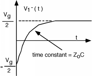 Figure \(\PageIndex{13}\): Reflected voltage as a function of time
The capacitor starts off looking like a short circuit, and charges up to look like an open circuit, which makes perfect sense. Can you figure out what the shape would be of a pulse reflected off of the capacitor, given that the time constant \(Z_{0} C\) was short compared to the width of the pulse?