
5.11: Combiners and Dividers
- Page ID
- 41115
\( \newcommand{\vecs}[1]{\overset { \scriptstyle \rightharpoonup} {\mathbf{#1}} } \)
\( \newcommand{\vecd}[1]{\overset{-\!-\!\rightharpoonup}{\vphantom{a}\smash {#1}}} \)
\( \newcommand{\id}{\mathrm{id}}\) \( \newcommand{\Span}{\mathrm{span}}\)
( \newcommand{\kernel}{\mathrm{null}\,}\) \( \newcommand{\range}{\mathrm{range}\,}\)
\( \newcommand{\RealPart}{\mathrm{Re}}\) \( \newcommand{\ImaginaryPart}{\mathrm{Im}}\)
\( \newcommand{\Argument}{\mathrm{Arg}}\) \( \newcommand{\norm}[1]{\| #1 \|}\)
\( \newcommand{\inner}[2]{\langle #1, #2 \rangle}\)
\( \newcommand{\Span}{\mathrm{span}}\)
\( \newcommand{\id}{\mathrm{id}}\)
\( \newcommand{\Span}{\mathrm{span}}\)
\( \newcommand{\kernel}{\mathrm{null}\,}\)
\( \newcommand{\range}{\mathrm{range}\,}\)
\( \newcommand{\RealPart}{\mathrm{Re}}\)
\( \newcommand{\ImaginaryPart}{\mathrm{Im}}\)
\( \newcommand{\Argument}{\mathrm{Arg}}\)
\( \newcommand{\norm}[1]{\| #1 \|}\)
\( \newcommand{\inner}[2]{\langle #1, #2 \rangle}\)
\( \newcommand{\Span}{\mathrm{span}}\) \( \newcommand{\AA}{\unicode[.8,0]{x212B}}\)
\( \newcommand{\vectorA}[1]{\vec{#1}} % arrow\)
\( \newcommand{\vectorAt}[1]{\vec{\text{#1}}} % arrow\)
\( \newcommand{\vectorB}[1]{\overset { \scriptstyle \rightharpoonup} {\mathbf{#1}} } \)
\( \newcommand{\vectorC}[1]{\textbf{#1}} \)
\( \newcommand{\vectorD}[1]{\overrightarrow{#1}} \)
\( \newcommand{\vectorDt}[1]{\overrightarrow{\text{#1}}} \)
\( \newcommand{\vectE}[1]{\overset{-\!-\!\rightharpoonup}{\vphantom{a}\smash{\mathbf {#1}}}} \)
\( \newcommand{\vecs}[1]{\overset { \scriptstyle \rightharpoonup} {\mathbf{#1}} } \)
\( \newcommand{\vecd}[1]{\overset{-\!-\!\rightharpoonup}{\vphantom{a}\smash {#1}}} \)
\(\newcommand{\avec}{\mathbf a}\) \(\newcommand{\bvec}{\mathbf b}\) \(\newcommand{\cvec}{\mathbf c}\) \(\newcommand{\dvec}{\mathbf d}\) \(\newcommand{\dtil}{\widetilde{\mathbf d}}\) \(\newcommand{\evec}{\mathbf e}\) \(\newcommand{\fvec}{\mathbf f}\) \(\newcommand{\nvec}{\mathbf n}\) \(\newcommand{\pvec}{\mathbf p}\) \(\newcommand{\qvec}{\mathbf q}\) \(\newcommand{\svec}{\mathbf s}\) \(\newcommand{\tvec}{\mathbf t}\) \(\newcommand{\uvec}{\mathbf u}\) \(\newcommand{\vvec}{\mathbf v}\) \(\newcommand{\wvec}{\mathbf w}\) \(\newcommand{\xvec}{\mathbf x}\) \(\newcommand{\yvec}{\mathbf y}\) \(\newcommand{\zvec}{\mathbf z}\) \(\newcommand{\rvec}{\mathbf r}\) \(\newcommand{\mvec}{\mathbf m}\) \(\newcommand{\zerovec}{\mathbf 0}\) \(\newcommand{\onevec}{\mathbf 1}\) \(\newcommand{\real}{\mathbb R}\) \(\newcommand{\twovec}[2]{\left[\begin{array}{r}#1 \\ #2 \end{array}\right]}\) \(\newcommand{\ctwovec}[2]{\left[\begin{array}{c}#1 \\ #2 \end{array}\right]}\) \(\newcommand{\threevec}[3]{\left[\begin{array}{r}#1 \\ #2 \\ #3 \end{array}\right]}\) \(\newcommand{\cthreevec}[3]{\left[\begin{array}{c}#1 \\ #2 \\ #3 \end{array}\right]}\) \(\newcommand{\fourvec}[4]{\left[\begin{array}{r}#1 \\ #2 \\ #3 \\ #4 \end{array}\right]}\) \(\newcommand{\cfourvec}[4]{\left[\begin{array}{c}#1 \\ #2 \\ #3 \\ #4 \end{array}\right]}\) \(\newcommand{\fivevec}[5]{\left[\begin{array}{r}#1 \\ #2 \\ #3 \\ #4 \\ #5 \\ \end{array}\right]}\) \(\newcommand{\cfivevec}[5]{\left[\begin{array}{c}#1 \\ #2 \\ #3 \\ #4 \\ #5 \\ \end{array}\right]}\) \(\newcommand{\mattwo}[4]{\left[\begin{array}{rr}#1 \amp #2 \\ #3 \amp #4 \\ \end{array}\right]}\) \(\newcommand{\laspan}[1]{\text{Span}\{#1\}}\) \(\newcommand{\bcal}{\cal B}\) \(\newcommand{\ccal}{\cal C}\) \(\newcommand{\scal}{\cal S}\) \(\newcommand{\wcal}{\cal W}\) \(\newcommand{\ecal}{\cal E}\) \(\newcommand{\coords}[2]{\left\{#1\right\}_{#2}}\) \(\newcommand{\gray}[1]{\color{gray}{#1}}\) \(\newcommand{\lgray}[1]{\color{lightgray}{#1}}\) \(\newcommand{\rank}{\operatorname{rank}}\) \(\newcommand{\row}{\text{Row}}\) \(\newcommand{\col}{\text{Col}}\) \(\renewcommand{\row}{\text{Row}}\) \(\newcommand{\nul}{\text{Nul}}\) \(\newcommand{\var}{\text{Var}}\) \(\newcommand{\corr}{\text{corr}}\) \(\newcommand{\len}[1]{\left|#1\right|}\) \(\newcommand{\bbar}{\overline{\bvec}}\) \(\newcommand{\bhat}{\widehat{\bvec}}\) \(\newcommand{\bperp}{\bvec^\perp}\) \(\newcommand{\xhat}{\widehat{\xvec}}\) \(\newcommand{\vhat}{\widehat{\vvec}}\) \(\newcommand{\uhat}{\widehat{\uvec}}\) \(\newcommand{\what}{\widehat{\wvec}}\) \(\newcommand{\Sighat}{\widehat{\Sigma}}\) \(\newcommand{\lt}{<}\) \(\newcommand{\gt}{>}\) \(\newcommand{\amp}{&}\) \(\definecolor{fillinmathshade}{gray}{0.9}\)Combiners are used to combine power from two or more sources. A typical use is to combine power from two high power amplifiers to obtain a higher power than would be otherwise be available. Dividers divide power so that the power from an amplifier can be routed to different parts of a circuit.
5.11.1 Wilkinson Combiner and Divider
The Wilkinson divider can be used as a combiner or divider that divides input power among the output ports [25]. Figure 5.10.4(a) is a two-way divider that splits the power at Port \(\mathsf{1}\) equally between the two output ports at Ports \(\mathsf{2}\) and \(\mathsf{3}\). A particular insight that Wilkinson brought was the introduction of the resistor between the output ports and this acts to suppress any imbalance between the output signals due to nonidealities. If the division is exact, no current will flow in the resistor. The circuit works less well as a general purpose combiner. Ideally power entering Ports \(\mathsf{2}\) and \(\mathsf{3}\) would combine losslessly and appear at Port \(\mathsf{1}\). A typical application is to combine the power at the output of two matched transistors where the amplitude and the phase
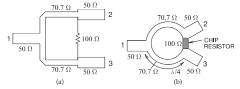
Figure \(\PageIndex{1}\): Wilkinson combiner and divider: (a) microstrip realization; and (b) higher performance microstrip implementation.
of the signals can be expected to be closely matched. However, if the signals are not identical, power will be absorbed in the resistor. The bandwidth of the Wilkinson combiner/divider is limited by the one-quarter wavelength long lines. However, the bandwidth is relatively large, approaching \(\pm 50\%\) [25]. Arbitrary power ratios can also be obtained [26, 27, 28].
The operation of the Wilkinson divider can be seen by deriving the input impedance of the two-way Wilkinson divider driven at Port \(\mathsf{1}\) (see Figure 5.10.4(e)). Since the Wilkinson divider is driven, the signals at Ports \(\mathsf{2}\) and \(\mathsf{3}\) will be identical, so it is as though the resistor in the Wilkinson divider is not there. The input impedance of one of the one-quarter wavelength long sections in Figure 5.10.4(e) is
\[\label{eq:1}Z_{1}=\frac{(\sqrt{2}Z_{0})^{2}}{Z_{0}}=2Z_{0} \]
and so the Wilkinson model reduces to that in Figure 5.10.4(f). The two \(2Z_{0}\) resistors are in parallel, resulting in the further model reductions in Figures 5.10.4(g) and 5.10.4(h). Thus Port \(\mathsf{1}\) is matched. A similar analysis shows that Ports \(\mathsf{2}\) and \(\mathsf{3}\) are matched (have an input impedance of \(Z_{0}\)). The \(S\) parameters of the two-way Wilkinson power divider with an equal split of the output power are therefore
\[\label{eq:2}\mathbf{S}=\left[\begin{array}{ccc}{0}&{-\jmath /\sqrt{2}}&{-\jmath /\sqrt{2}}\\{-\jmath /\sqrt{2}}&{0}&{0}\\{-\jmath/\sqrt{2}}&{0}&{0}\end{array}\right] \]
Figure 5.10.4(b) is a compact representation of the two-way Wilkinson divider, and a three-way Wilkinson divider is shown in Figure 5.10.4(d). This pattern can be repeated to produce \(N\)-way power dividing. The lumped-element version of the Wilkinson divider shown in Figure 5.10.4(c) is based on the \(LC\) model of a one-quarter wavelength long transmission line segment. With a \(50\:\Omega\) system impedance and center frequency of \(400\text{ MHz}\), the elements of the lumped element are (from Figure 2-37(c)) \(L = 28.13\text{ nH, }C_{1} = 11.25\text{ pF, }C_{2} = 5.627\text{ pF,}\) and \(R = 100\:\Omega\).
Figure \(\PageIndex{1}\)(a) is the layout of a direct microstrip realization of a Wilkinson divider. The obvious problem is how to incorporate the resistor. As long as the resistor is placed symmetrically this is not as severe a problem as it would initially seem, as power is not dissipated in the resistor unless there is an imbalance. A higher-performance microstrip layout is shown in Figure \(\PageIndex{1}\)(b), where the transmission lines are curved to bring the output ports near each other so that a chip resistor can be used.
Example \(\PageIndex{1}\): Lumped-Element Wilkinson Divider
Design a lumped-element 2-way Wilkinson divider in a \(60\:\Omega\) system. The center frequency of the design should be \(10\text{ GHz}\).
Solution
The design begins with the transmission line form of the Wilkinson divider which will be converted to a lumped-element form latter. The design parameters are \(Z_{0} = 60\:\Omega,\) \(f = 10\text{ GHz, }\)\(\omega = 2\pi 10^{10} = 2.283\cdot 10^{10}\text{ rads/s}\) and so
\[Z_{01}=\sqrt{2}Z_{0}=84.85\:\Omega,\quad R=2Z_{0}=120\:\Omega\nonumber \]
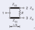
Figure \(\PageIndex{2}\)
The next stage is to convert the transmission lines to lumped elements. A broadband design of a quarter-wavelength transmission line was presented in Figure 2-37(b) of [15]. That is, each of the quarter-wave lines has the model
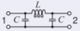
Figure \(\PageIndex{3}\)
with
\[\begin{aligned} L &= Z_{01}/\omega = 84.85/\omega = 954.9\text{ pH}\nonumber \\ C &= 1/(Z_{01}\omega )=1/(84.85\omega ) = 265.3\text{ fF}\nonumber\end{aligned}\nonumber \]
So the final lumped element design is
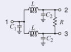
Figure \(\PageIndex{4}\)
with
\[\begin{aligned} C_{1}&=2C=530.6\text{ fF}\nonumber \\ C_{2}&=C=265.3\text{ fF}\nonumber \\ L&=954.9\text{ pH}\nonumber \\ R&=120\:\Omega\nonumber\end{aligned}\nonumber \]
5.11.2 Chireix Combiner
One of the problems with the Wilkinson structure when it is used as a combiner is that it is only efficient at combining when the two signals to be combined are in phase. A better combiner is the Chireix combiner [29] shown in Figure 5.12.1. This combiner is often used when combining the outputs of two amplifiers achieving efficient combining even when the signals to be combined are not identical [30, 31, 32, 33].