
5.12: Transmission Line Transformer
- Page ID
- 41116
\( \newcommand{\vecs}[1]{\overset { \scriptstyle \rightharpoonup} {\mathbf{#1}} } \)
\( \newcommand{\vecd}[1]{\overset{-\!-\!\rightharpoonup}{\vphantom{a}\smash {#1}}} \)
\( \newcommand{\id}{\mathrm{id}}\) \( \newcommand{\Span}{\mathrm{span}}\)
( \newcommand{\kernel}{\mathrm{null}\,}\) \( \newcommand{\range}{\mathrm{range}\,}\)
\( \newcommand{\RealPart}{\mathrm{Re}}\) \( \newcommand{\ImaginaryPart}{\mathrm{Im}}\)
\( \newcommand{\Argument}{\mathrm{Arg}}\) \( \newcommand{\norm}[1]{\| #1 \|}\)
\( \newcommand{\inner}[2]{\langle #1, #2 \rangle}\)
\( \newcommand{\Span}{\mathrm{span}}\)
\( \newcommand{\id}{\mathrm{id}}\)
\( \newcommand{\Span}{\mathrm{span}}\)
\( \newcommand{\kernel}{\mathrm{null}\,}\)
\( \newcommand{\range}{\mathrm{range}\,}\)
\( \newcommand{\RealPart}{\mathrm{Re}}\)
\( \newcommand{\ImaginaryPart}{\mathrm{Im}}\)
\( \newcommand{\Argument}{\mathrm{Arg}}\)
\( \newcommand{\norm}[1]{\| #1 \|}\)
\( \newcommand{\inner}[2]{\langle #1, #2 \rangle}\)
\( \newcommand{\Span}{\mathrm{span}}\) \( \newcommand{\AA}{\unicode[.8,0]{x212B}}\)
\( \newcommand{\vectorA}[1]{\vec{#1}} % arrow\)
\( \newcommand{\vectorAt}[1]{\vec{\text{#1}}} % arrow\)
\( \newcommand{\vectorB}[1]{\overset { \scriptstyle \rightharpoonup} {\mathbf{#1}} } \)
\( \newcommand{\vectorC}[1]{\textbf{#1}} \)
\( \newcommand{\vectorD}[1]{\overrightarrow{#1}} \)
\( \newcommand{\vectorDt}[1]{\overrightarrow{\text{#1}}} \)
\( \newcommand{\vectE}[1]{\overset{-\!-\!\rightharpoonup}{\vphantom{a}\smash{\mathbf {#1}}}} \)
\( \newcommand{\vecs}[1]{\overset { \scriptstyle \rightharpoonup} {\mathbf{#1}} } \)
\( \newcommand{\vecd}[1]{\overset{-\!-\!\rightharpoonup}{\vphantom{a}\smash {#1}}} \)
\(\newcommand{\avec}{\mathbf a}\) \(\newcommand{\bvec}{\mathbf b}\) \(\newcommand{\cvec}{\mathbf c}\) \(\newcommand{\dvec}{\mathbf d}\) \(\newcommand{\dtil}{\widetilde{\mathbf d}}\) \(\newcommand{\evec}{\mathbf e}\) \(\newcommand{\fvec}{\mathbf f}\) \(\newcommand{\nvec}{\mathbf n}\) \(\newcommand{\pvec}{\mathbf p}\) \(\newcommand{\qvec}{\mathbf q}\) \(\newcommand{\svec}{\mathbf s}\) \(\newcommand{\tvec}{\mathbf t}\) \(\newcommand{\uvec}{\mathbf u}\) \(\newcommand{\vvec}{\mathbf v}\) \(\newcommand{\wvec}{\mathbf w}\) \(\newcommand{\xvec}{\mathbf x}\) \(\newcommand{\yvec}{\mathbf y}\) \(\newcommand{\zvec}{\mathbf z}\) \(\newcommand{\rvec}{\mathbf r}\) \(\newcommand{\mvec}{\mathbf m}\) \(\newcommand{\zerovec}{\mathbf 0}\) \(\newcommand{\onevec}{\mathbf 1}\) \(\newcommand{\real}{\mathbb R}\) \(\newcommand{\twovec}[2]{\left[\begin{array}{r}#1 \\ #2 \end{array}\right]}\) \(\newcommand{\ctwovec}[2]{\left[\begin{array}{c}#1 \\ #2 \end{array}\right]}\) \(\newcommand{\threevec}[3]{\left[\begin{array}{r}#1 \\ #2 \\ #3 \end{array}\right]}\) \(\newcommand{\cthreevec}[3]{\left[\begin{array}{c}#1 \\ #2 \\ #3 \end{array}\right]}\) \(\newcommand{\fourvec}[4]{\left[\begin{array}{r}#1 \\ #2 \\ #3 \\ #4 \end{array}\right]}\) \(\newcommand{\cfourvec}[4]{\left[\begin{array}{c}#1 \\ #2 \\ #3 \\ #4 \end{array}\right]}\) \(\newcommand{\fivevec}[5]{\left[\begin{array}{r}#1 \\ #2 \\ #3 \\ #4 \\ #5 \\ \end{array}\right]}\) \(\newcommand{\cfivevec}[5]{\left[\begin{array}{c}#1 \\ #2 \\ #3 \\ #4 \\ #5 \\ \end{array}\right]}\) \(\newcommand{\mattwo}[4]{\left[\begin{array}{rr}#1 \amp #2 \\ #3 \amp #4 \\ \end{array}\right]}\) \(\newcommand{\laspan}[1]{\text{Span}\{#1\}}\) \(\newcommand{\bcal}{\cal B}\) \(\newcommand{\ccal}{\cal C}\) \(\newcommand{\scal}{\cal S}\) \(\newcommand{\wcal}{\cal W}\) \(\newcommand{\ecal}{\cal E}\) \(\newcommand{\coords}[2]{\left\{#1\right\}_{#2}}\) \(\newcommand{\gray}[1]{\color{gray}{#1}}\) \(\newcommand{\lgray}[1]{\color{lightgray}{#1}}\) \(\newcommand{\rank}{\operatorname{rank}}\) \(\newcommand{\row}{\text{Row}}\) \(\newcommand{\col}{\text{Col}}\) \(\renewcommand{\row}{\text{Row}}\) \(\newcommand{\nul}{\text{Nul}}\) \(\newcommand{\var}{\text{Var}}\) \(\newcommand{\corr}{\text{corr}}\) \(\newcommand{\len}[1]{\left|#1\right|}\) \(\newcommand{\bbar}{\overline{\bvec}}\) \(\newcommand{\bhat}{\widehat{\bvec}}\) \(\newcommand{\bperp}{\bvec^\perp}\) \(\newcommand{\xhat}{\widehat{\xvec}}\) \(\newcommand{\vhat}{\widehat{\vvec}}\) \(\newcommand{\uhat}{\widehat{\uvec}}\) \(\newcommand{\what}{\widehat{\wvec}}\) \(\newcommand{\Sighat}{\widehat{\Sigma}}\) \(\newcommand{\lt}{<}\) \(\newcommand{\gt}{>}\) \(\newcommand{\amp}{&}\) \(\definecolor{fillinmathshade}{gray}{0.9}\)One of the challenges in RF engineering is achieving broadband operation of transformers from megahertz up to several gigahertz. In this section, several structures are presented that operate as magnetic transformers at frequencies below several hundred megahertz but as coupled transmission line structures at high frequencies. A transformer that achieves this and,
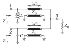
Figure \(\PageIndex{1}\): Chireix combiner.
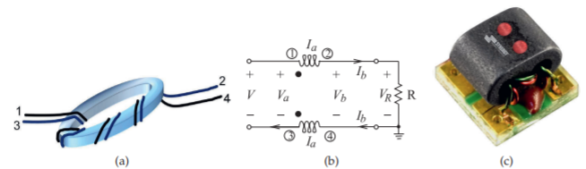
Figure \(\PageIndex{2}\): A broadband RF balun as coupled lines wound around a ferrite core: (a) physical realization (the wires \(1–2\) and \(3–4\) form a single transmission line); (b) equivalent circuit using a wire-wound transformer (the number of primary and secondary windings are equal); and (c) packaged as a module (Model TM1-9 with a frequency range of \(100–5000\text{ MHz}\). Copyright Synergy Microwave Corporation, used with permission [34]).
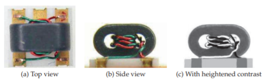
Figure \(\PageIndex{3}\): Open-core surface-mount transformer. Copyright 2012 Scientific Components Corporation d/b/a Mini-Circuits, used with permission [11].
in this configuration, realizes a balun is shown in Figure \(\PageIndex{2}\)(a). Below a few hundred megahertz this functions as a magnetic transformer. Above this frequency the ferrite core cannot respond to the signal and the magnetic circuit through the core appears as an open circuit. Then, since the transformer is not operating as a magnetic transformer anymore, magnetic leakage is inconsequential. At high frequencies the wire transmission lines are closely coupled and appear as a perfect coupler if the lines (or wires here) are long enough. The equivalent circuit of this structure is shown in Figure \(\PageIndex{2}\)(b). At high frequencies, stray capacitances between the windings becomes important but become part of the transmission line capacitance. Many types of transformers operating from several megahertz to several gigahertz can be realized using the same principle and are available as surface-mount components (see Figure \(\PageIndex{2}\)(c)).
High-frequency coupling is enhanced by twisting the conductors as shown in Figure \(\PageIndex{3}\). The combination of magnetic coupling at low frequencies with transmission line coupling at high frequencies yields a transformer that operates over very wide bandwidths.
5.12.1 Transmission Line Transformer as a Balun
The schematic of a broadband \(1:1\) RF balun is shown in Figure \(\PageIndex{2}\)(b) and a realization of it is shown in Figure \(\PageIndex{2}\)(a and c). The \(1:1\) designation indicates that there is no impedance transformation. The circuit equations describing this balun are (from the \(ABCD\) parameters of a transmission line; see Table 2.2.1)
\[\label{eq:1} V_{a} = V_{b}\cos(\beta\ell ) + \jmath I_{b} Z_{0} \sin(\beta\ell)\quad\text{and}\quad I_{a} = I_{b}\cos(\beta\ell ) + \jmath\frac{V_{b}}{Z_{0}}\sin(\beta\ell) \]
and the load resistance creates a third equation,
\[\label{eq:2}V_{b}=I_{b}R \]
The aim in the following is the development of a design equation that describes the essential properties of the structure. Substituting Equation \(\eqref{eq:2}\) in Equation \(\eqref{eq:1}\) leads to
\[\label{eq:3}V_{a}=V_{b}\left[\cos(\beta\ell)+\jmath\frac{Z_{0}}{R}\sin(\beta\ell)\right]\quad\text{and}\quad I_{a}=\frac{V_{b}}{R}\left[\cos(\beta\ell)+\jmath\frac{R}{Z_{0}}\sin(\beta\ell)\right] \]
Choosing \(Z_{0} = R\) yields (since \(\text{e}^{\jmath\beta\ell} = \cos(\beta\ell) + \jmath\sin(\beta\ell)\))
\[\label{eq:4}V_{a}=V_{b}\text{e}^{\jmath\beta\ell}\quad\text{and}\quad I_{a}=(V_{b}/R)\text{e}^{\jmath\beta\ell} \]
and so
\[\label{eq:5}Z_{\text{in}}=V_{a}/I_{a}=R \]
This analysis is idealized, as parasitics are eliminated (mainly parasitic capacitances), but the above equation indicates that the essential function of the structure is that of a balun with no impedance transformation. The transformer arrangement shown in Figure \(\PageIndex{2}\)(b) is of particular interest as it can be realized using coupled transmission lines.
5.12.2 \(4:1\) Impedance Transformer at High Frequencies
By changing the connection of the transformer terminals it is possible to achieve impedance transformation. A \(4:1\) impedance transformer is shown in Figure \(\PageIndex{4}\)(a). A specific arrangement of the primary and secondary windings puts this into what is called the transmission line form, shown in Figure \(\PageIndex{5}\). At high frequencies port conditions are enforced so that the currents at Ports \(\mathsf{1}\) and \(\mathsf{3}\) (and at Ports \(\mathsf{2}\) and \(\mathsf{4}\)) are matched, as shown in Figure \(\PageIndex{5}\). Showing that \(Z_{\text{in}} = R\) begins with
\[\label{eq:6}\begin{array}{ll}{V_{a} = V_{b} \cos(\beta\ell ) + \jmath I_{b}Z_{0} \sin(\beta\ell )}&{I_{a} = I_{b} \cos(\beta\ell) + \jmath \frac{V_{b}}{Z_{0}} \sin(\beta\ell )}\\{V_{\text{in}}=V_{a}+R(I_{a}+I_{b}),\quad\text{and}}&{V_{b}=(I_{a}+I_{b})R}\end{array} \]
So the aim is to find \(Z_{\text{in}} = V_{\text{in}}/I_{a}\), as this defines the required electrical function. Now
\[\label{eq:7}V_{\text{in}}=V_{a}+V_{b}=V_{b}[1+\cos(\beta\ell)]+\jmath I_{b}Z_{0}\sin(\beta\ell) \]
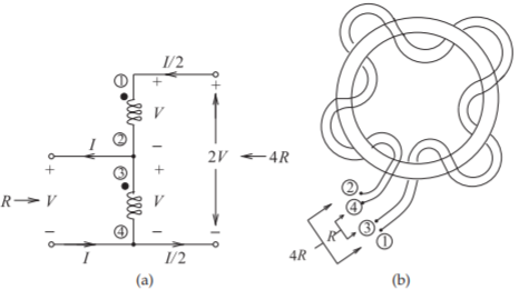
Figure \(\PageIndex{4}\): A \(4:1\) impedance transformer: (a) Schematic (the coils have the same number of windings); and (b) realization as transformer with twisted coupled wires twisted around a magnetic core.
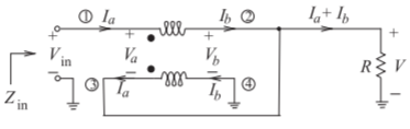
Figure \(\PageIndex{5}\): A transmission line form of the \(4:1\) impedance transformer of Figure \(\PageIndex{4}\), after [35]. (The number of primary and secondary windings are the same.)
and using the equations above
\[\begin{align}I_{a}&=I_{b}\cos(\beta\ell)+\jmath(I_{a}+I_{b})\frac{R}{Z_{0}}\sin(\beta\ell)\nonumber \\ \label{eq:8}I_{b}&=I_{a}\frac{Z_{0}-\jmath R\sin(\beta\ell)}{Z_{0}\cos(\beta\ell)+\jmath R\sin(\beta\ell)}\end{align} \]
Thus
\[\label{eq:9}Z_{\text{in}}=\frac{V_{\text{in}}}{I_{a}}=Z_{0}\frac{2R[1 + \cos(\beta\ell)] + \jmath Z_{0} \sin(\beta\ell)}{Z_{0} \cos(\beta\ell) + \jmath R \sin(\beta\ell )} \]
At very low frequencies the electrical length of the transmission line, \(\beta\ell\), is negligibly small and \(Z_{\text{in}} = 4R\). To see what happens when the length of the transmission line has a significant effect, consider the special case when \(Z_{0} = 2R\), then
\[\label{eq:10}Z_{\text{in}}=2R(1+\text{e}^{-\jmath\beta\ell}) \]
For a short line, that is, \(\ell < 0.1\lambda\) or \(\beta\ell < 0.2\pi\), Equation \(\eqref{eq:10}\) can be approximated as
\[\label{eq:11}Z_{\text{in}}\approx 2R[1+1-\jmath\beta\ell]=4R-\jmath R(2\beta\ell) \]
The imaginary component, \(−\jmath R2\beta\ell\), is a capacitance and it must be resonated out (e.g., by a series inductor) to obtain the required resistance transformation.
The general approach described above can be used to design transformers with higher impedance ratios. Two more, a \(9:1\) transformer and a \(16:1\) transformer, are shown in Figure \(\PageIndex{6}\).
A practical broadband transmission line realization of the \(4:1\) transformer is shown in Figure \(\PageIndex{4}\)(b), where the transmission line is a pair of twisted wires.
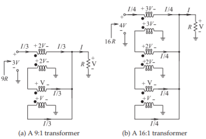
Figure \(\PageIndex{6}\): High-order impedance transformers.
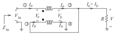
Figure \(\PageIndex{7}\): Low-frequency schematic of the \(4:1\) impedance transformer shown in Figure \(\PageIndex{4}\)(a).
5.12.3 \(4:1\) Impedance Transformer at Low Frequencies
In the previous section it was shown that the impedance transformer in Figure \(\PageIndex{4}\)(a) acts as a \(4:1\) impedance transformer at high frequencies where the structure can be considered to be a transmission line. In this section it will be shown that the transformer is also a \(4:1\) impedance transformer at low frequencies where the structure can be considered to be a wire-wound transformer.
At low frequencies, the port conditions\(^{1}\) at the ends of the transmission line are not enforced and so a better low frequency representation of the transformer currents is shown in Figure \(\PageIndex{7}\). If at low frequencies the transformer of Figure \(\PageIndex{5}\) has a self-inductance of \(L_{s}\) and a mutual inductance of \(M\), then the circuit equations for the transformer are
\[\begin{align}\label{eq:12}V_{\text{in}}-V_{b}&=\jmath\omega L_{s}I_{a}-\jmath\omega MI_{b}\\ \label{eq:13}V_{b}&=-\jmath\omega L_{s}I_{b}+\jmath\omega MI_{a} \\ \label{eq:14}V_{b}&=(I_{a}+I_{b})R\end{align} \]
Equating Equations \(\eqref{eq:13}\) and \(\eqref{eq:14}\) and rearranging,
\[\label{eq:15}I_{b}=-\left(\frac{R-\jmath\omega M}{R+\jmath\omega L_{s}}\right)I_{a} \]
Combining Equations \(\eqref{eq:12}\) and \(\eqref{eq:14}\) and rearranging,
\[\label{eq:16}V_{\text{in}}=(R+\jmath\omega L_{s})I_{a}+(R-\jmath\omega M)I_{b} \]
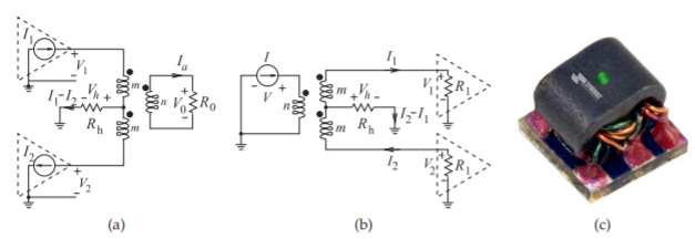
Figure \(\PageIndex{8}\): A \(180^{\circ}\) hybrid transformer: (a) used as a combiner; (b) used as a splitter; and (c) center-tapped transformer as a surface-mount component (Model TM1-2 with a frequency range of \(20–1200\text{ MHz}\). Copyright Synergy Microwave Corporation, used with permission [34]).
Replacing \(I_{b}\) in Equation \(\eqref{eq:16}\) using Equation \(\eqref{eq:15}\) yields
\[\label{eq:17}V_{\text{in}}=\left[(R+\jmath\omega L_{s})-\frac{(R-\jmath\omega M)^{2}}{R+\jmath\omega L_{s}}\right]I_{a} \]
Thus the input impedance is
\[\label{eq:18}Z_{\text{in}}=\frac{V_{\text{in}}}{I_{a}}=\frac{R^{2} + \jmath 2R\omega L_{s} − (\omega L_{s})^{2} − R^{2} + \jmath 2R\omega M + (\omega M)^{2}}{R+\jmath\omega L_{s}} \]
If ideal coupling is assumed (i.e., \(M = L_{s}\)) then Equation \(\eqref{eq:18}\) reduces to
\[\label{eq:19}Z_{\text{in}}=\frac{\jmath 4R\omega L_{s}}{R+\jmath\omega L_{s}} \]
If \(\jmath\omega L_{s} ≫ R\), then
\[\label{eq:20}Z_{\text{in}}\approx 4R \]
Thus the transformer is a \(4:1\) impedance transformer both at low frequencies when the structure acts as a magnetic transformer and, as seen in Section 5.12.2, at higher frequencies when the structure acts like a transmission line. Design of the impedance transformer is then directed at managing the frequency transition region and ensuring that the required impedance transformation occurs there as well. In practice, very broadband operation is not difficult to achieve.
5.12.4 Hybrid Transformer Used as a Combiner
In Figure \(\PageIndex{8}\)(a) a \(180^{\circ}\) hybrid transformer is used to combine the outputs of two power amplifiers that are driven \(180^{\circ}\) out of phase with respect to each other. This is commonly done when the power available from just one solid-state transistor amplifier is not sufficient to meet power requirements. Since the sum of the amp-turns of an ideal transformer must be zero,
\[\label{eq:21}nI_{o}=m(I_{1}+I_{2}) \]
Example \(\PageIndex{1}\): Transformer Design
The Thevenin equivalent output impedance of each amplifier in Figure \(\PageIndex{8}\)(a) is \(1\:\Omega\) and the system impedance, \(R_{0}\), is \(50\:\Omega\). Choose the transformer windings for maximum power transfer.
Solution
For maximum power transfer, \(R_{\text{in}} = 1\:\Omega\), and so from Equation \(\eqref{eq:21}\),
\[\label{eq:22}1=\left(\frac{m}{n}\right)^{2}\cdot 2\cdot 50\quad\text{and}\quad\frac{m}{n}=0.1 \]
Thus with a \(10:1\) winding ratio the required impedance transformation can be achieved.
5.12.5 Hybrid Transformer Used as a Power Splitter
The hybrid transformer can also be used to split power from a source to drive two loads. The circuit of Figure \(\PageIndex{8}\)(b) splits power from a current source driver into two loads. With the number of primary and secondary windings equal (i.e., \(m = n\)), the circuit equations are
\[\label{eq:23}I = I_{1} + I_{2},\quad V_{1} = V + V_{h},\quad \text{and}\quad V_{2} = V_{h} − V \]
Thus
\[\label{eq:24}V_{1}-V_{h}=V_{h}-V_{2} \]
Using \(V_{1} = R_{1}I_{1},\: V_{2} = −I_{2}R_{2},\) and \(V_{h} = (I_{2} − I_{1})R_{h},\) the desired electrical characteristics of the splitter are obtained:
\[\label{eq:25}\frac{I_{2}}{I_{1}}=\frac{R_{1}+2R_{h}}{R_{2}+2R_{h}} \]
Several observations can be made about the performance of the power splitter. If \(R_{1} = R_{2}\), then \(I_{1} = I_{2}\) for any value of \(R_{h}\). Conversely, if \(R_{1}\neq R_{2},\: I_{1}\neq I_{2}\) for a finite \(R_{h}\). To obtain equal drive currents in both power amplifiers in spite of variations in \(R_{1}\) and \(R_{2}\), the center tap of the transformer needs to be omitted so that \(R_{h} = ∞\).
5.12.6 Broadband Hybrid Combiner
A broadband hybrid combiner is shown in Figure \(\PageIndex{9}\). In what follows, it is shown that this combiner has the property of accommodating mismatches of the amplifiers. The development begins by assuming that the transformers have an equal number of turns on each winding. These two transformers are used to make a broadband (transmission line transformer) hybrid coupler. The circuit equations are
\[\begin{align} \label{eq:26}I_{1}=I_{a}+I_{b}\quad &\text{and}\quad I_{2}=I_{a}-I_{b} \\ \label{eq:27} I_{a}=\frac{1}{2}(I_{1}+I_{2})\quad &\text{and}\quad I_{b}=\frac{1}{2}(I_{1}-I_{2}) \\ \label{eq:28}V_{1}=\frac{V_{o}}{2}+V_{h}\quad &\text{and}\quad V_{2}=\frac{V_{o}}{2}-V_{h}\end{align} \]
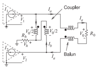
Figure \(\PageIndex{9}\): Broadband hybrid power combiner.
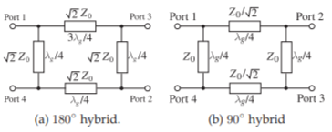
Figure \(\PageIndex{10}\): Topologies of ring-type hybrids.
Thus
\[\begin{align}\label{eq:29}\frac{V_{1}}{I_{1}}&=R_{h}\left(1-\frac{I_{2}}{I_{1}}\right)+\frac{R_{0}}{2}\left(1-\frac{I_{2}}{I_{1}}\right) \\ \label{eq:30}\frac{V_{2}}{I_{2}}&=\frac{R_{0}}{2}\left(1+\frac{I_{1}}{I_{2}}\right)-R_{h}\left(\frac{I_{1}}{I_{2}}-1\right)\end{align} \]
A special situation is when \(R_{h} = R_{0}/2\), and then \(V_{2}/I_{2} = R_{0}\) and \(V_{1}/I_{1} = R_{0}\). Thus each of the amplifiers sees a constant load resistance, \(R_{0}\), even if the amplifiers are mismatched, resulting, for example, when the amplifiers have slightly different gains.
Footnotes
[1] Currents at the pair of terminals of a port are equal in magnitude and opposite in direction.