
2.17: Active Filters
- Page ID
- 46083
With active circuits, losses in lumped-element components can be compensated for by the gain of active devices resulting in filters with high \(Q\). Inverters can also be realized efficiently. The net result is that active filters provide a performance per unit area advantage over passive element realizations. Of course, active filters are limited to low-level signals (such as in the receive circuitry, and prior to the power amplifier stages) as the full power of the signal must be handled by the active devices in the active filter. With active devices, additional noise is introduced and so the noise figure of an active filter must be considered at RF where bandwidths are significant.
At microwave frequencies active filters based on traditional low-frequency concepts have relatively low \(Q\). Higher \(Q\) and narrower-band applications require active inductors or distributed techniques. The smallest active filters are the ones that use active inductors and the largest use distributed transmission line elements.
Sometimes the main role of a filter is to limit the dynamic range of signals presented to active circuits, thereby limiting distortion. Clearly active filters are not suitable when large out-of-band signals are a concern.
2.17.1 Radio Frequency Active Filters
There are several problems with lumped-element filters. High-order filters require many poles and zeros that must be precisely placed, requiring small tolerances. With active filters it is possible, to some degree, to achieve higher-order filters with fewer reactive elements and so the tolerancing problem is considerably reduced. Also, there are a few designs that can be tuned electronically. Lumped-element bandpass filters and highpass filters require inductors. Inductors are a major problem, as RF inductors are lossy and also only relatively small values can be obtained. On-chip inductors take considerable area and can thereby dominate the cost of RFICs. With active filters, feedback and capacitors can be used to realize inductor-like characteristics, defined as a positive imaginary impedance increasing with frequency at least over a small frequency range. Many times, and especially at lower radio frequencies, lumped inductors are no longer required. The size of capacitors in filters is another issue, and using feedback and gain, the effective value of capacitors can be magnified. All this comes with limits. The principle limit is that the cutoff frequency of the transistors must be much higher than the operating frequency of the filters. This is a cost incurred whenever feedback is used. A rough rule of thumb is that the transistor cutoff frequency should be about \(10\) times the operating frequency. So for a \(5\text{ GHz}\) bandpass filter, a \(50\text{ GHz}\) transistor process is required. The other significant cost is that active filters are only suitable for small signals. The efficiency, a measure of the amount of DC power used in producing the RF output signal, is then not a consideration. Active filters cannot be used where signal levels are likely to be large (such as at the output of a power amplifier or at the receiver input, due to likely out-of-band signals).
The essential aspect of low-RF active filters is the use of feedback, with reactive feedback elements, to realize a frequency-domain transfer function with poles and zeros. The aim is not to synthesize effective capacitors and inductors, but to focus on the overall response. Active filters are generally developed as stages, with each stage realizing a second- or higher-order transfer function. Design is simulation driven, as this is the only way to account for the active device parasitics.
In operational amplifier design, feedback is used to achieve gain stability, but at the cost of reduced bandwidth. If reactive feedback elements are used, high-order transfer functions can be obtained with just a few reactive elements. In Figure \(\PageIndex{1}\), a twin-T notch network is connected in the operational amplifier feedback path to obtain a bandpass filter [27]. Away from the notch frequency the feedback path has a high impedance and the overall amplifier gain falls off. As the signal frequency approaches the notch frequency, the feedback path becomes effective and the amplifier gain increases. The notch frequency, \(f_{n}\), is proportional to the RC product of the feedback components and the \(Q\) is proportional to the amplifier gain. The governing equations for this filter are
\[\label{eq:1}f_{n}=1/(2\pi RC)\quad\text{and}\quad Q=(1+G)/4 \]
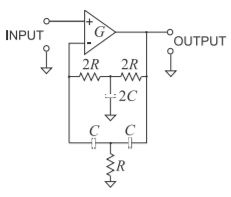
Figure \(\PageIndex{1}\): Active twin-T bandpass filter: center frequency \(f_{0} = \pi RC/4\) and \(Q = (G + 1)/4\).
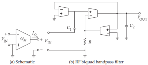
Figure \(\PageIndex{2}\): Operational transconductance amplifier with transconductance \(G_{M}\). In (a) \(I_{O} = G_{M}V_{\text{IN}}\).
2.17.2 Biquadratic Filters
Biquadratic filters are an important class of filters and are the basic building block used in analog and RF active filters. Biquad filters commonly use operational transconductance amplifiers (OTAs), the schematic of which is shown in Figure \(\PageIndex{2}\)(a). Here \(I_{O} = G_{M} V_{\text{IN}}\), which is also the basic characteristic of an individual transistor. These circuits have characteristics typical of operational amplifiers, including gain stability and resistance to component tolerance variations. OTA-based filters have the advantage of easy tunability, with pole and zero frequencies electronically adjustable. An RF bandpass biquad filter is shown in Figure \(\PageIndex{2}\)(b). Stages such as this are cascaded to realize high-order filters.
Biquadratic filters implement the transfer function
\[\label{eq:2}H(s)=\frac{V_{\text{OUT}}}{V_{\text{IN}}} =\frac{N(s)}{D(s)}=\frac{a_{2}s^{2}+a_{1}s+a_{0}}{s^{2}+b_{1}s+b_{0}}=\frac{a_{2}(s+z_{1})(s+z_{2})}{(s+p_{1})(s+p_{2})} \]
This is referred to as a biquadratic function and filters that implement this function are called biquadratic filters or simply biquad filters. There are several special types of biquad filters.
The form of the biquadratic function for a second-order lowpass filter is
\[\label{eq:3}H_{\text{LP}}(s)=\frac{a_{0}}{s^{2}+b_{1}s+b_{0}}=\frac{K\omega_{p}^{2}}{s^{2}+(\omega_{p}/Q_{p})s+\omega_{p}^{2}} \]
\(H_{\text{LP}}(s)\) has a double zero at \(s =\infty\) and thus negligible response at very high frequencies.
The highpass form of the biquadratic filter is described by
\[\label{eq:4}H_{\text{HP}}(s)=\frac{a_{2}s^{2}}{s^{2}+b_{1}s+b_{0}}=\frac{Ks^{2}}{s^{2}+(\omega_{p}/Q_{p})s+\omega_{p}^{2}} \]
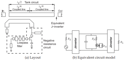
Figure \(\PageIndex{3}\): Active coupled distributed filter. After [30].
The response of \(H_{\text{HP}}(s)\) at high frequencies is \(K\) and the response at very low frequencies goes to zero.
The bandpass form of the biquadratic filter is described by
\[\label{eq:5}H_{\text{BP}}(s)=\frac{a_{1}s}{s^{2}+b_{1}s+b_{0}}=\frac{K(\omega_{p}/Q_{p})s}{s^{2}+(\omega_{p}/Q_{p})s+\omega_{p}^{2}} \]
The response of \(H_{\text{BP}}(s)\) at high and low frequencies goes to zero, and only at and near the center frequency, \(\omega =\omega_{p}\), is there a reasonable response.
The band-reject or notch form of the biquadratic filter is described by
\[\label{eq:6}H_{\text{BR}}(s)=\frac{a_{2}s^{2}+a_{0}}{s^{2}+b_{1}s+b_{0}}=\frac{K(s^{2}+\omega_{z}^{2})}{s^{2}+(\omega_{p}/Q_{p})s+\omega_{p}^{2}} \]
The response of \(H_{\text{BR}}(s)\) at high and low frequencies is high, but there is a double zero at the notch frequency, \(\omega =\omega_{z}\), where the response is very low.
With all of the biquadratic filters, the sharpness of the response is determined by \(Q_{p}\). The edge frequency or center frequency is \(\omega_{p}\) for the bandpass, lowpass, and highpass filters, and the notch frequency is \(\omega_{z}\) for the bandstop filter.
2.17.3 Distributed Active Filters
At high microwave frequencies, good results can be obtained by combining distributed elements with a gain stage. Commonly the active devices are used as coupling devices. A negative resistance can be produced using the active devices that can compensate for the losses associated with the transmission line elements or lumped passive elements in the filter. The concept uses a resonant tank circuit formed by a transmission line or lumped-element resonator with a negative resistance coupled into the tank circuit by the active devices [28, 29, 30]. This concept is illustrated in Figure \(\PageIndex{3}\). Here a one-half wavelength long resonator forms a resonant circuit (commonly called a tank circuit in this context). A negative resistance is coupled into the tank circuit to compensate for losses in the resonator and the result is effectively a lossless tank circuit.
An active resonator circuit is shown in Figure \(\PageIndex{4}\). The design of the lossless resonator is based on the negative resistance obtained when the capacitor is connected at the source of the MESFET. This element in the
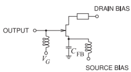
Figure \(\PageIndex{4}\): An active resonator circuit. After [31].
source provides a feedback path between the output of the circuit, the drain-to-ground voltage, and the input gate-to-source voltage. An increase in the drain-source current leads to a voltage at the source that changes the gate-source voltage. This induces a negative resistance that is adjusted through the feedback capacitance, \(C_{FB}\), to compensate for inductor losses. An additional inductor, \(L_{P}\), is added at the gate. The inductor resonates with the series combination of \(C_{FB}\) and \(C_{GS}\). \(C_{FB}\) can be implemented using a varactor diode to enable electronic tuning.