
2.3: Amplifier Gain Definitions
- Page ID
- 46025
As with all circuit design, a few figures of merit (FOMs) are used to guide design. The most important metric in amplifier design is the gain
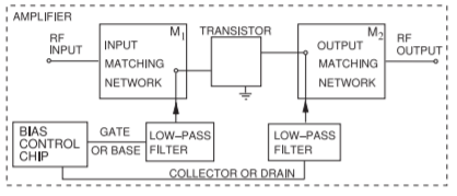
Figure \(\PageIndex{1}\): Block diagram of an RF amplifier including biasing networks.
Data Sheet Extract.
\[\begin{array}{ll}{\text{Transistor technology:}}&{\text{Depletion-mode pHEMT.}}\\{\text{Model:}}&{\text{FPD6836P70 from QORVO, Inc.}}\\{\text{Description:}}&{\text{Low-noise, high-frequency packaged pHEMT.}}\\{}&{\text{Optimized for low-noise, high-frequency applications.}}\\{\text{Synopsis:}}&{22\text{ dBm output power (P}1\text{ dB}).}\\{}&{15\text{ dB power gain (G}1\text{ dB) at }5.8\text{ GHz, Usable gain to }18\text{ GHz.}}\\{}&{0.8\text{ dB noise figure at }5.8\text{ GHz, }32\text{ dBm output IP3 at }5.8\text{ GHz.}}\\{}&{45\text{% power-added efficiency at }5.8\text{ GHz.}}\\{}&{\text{Usable gain to }18\text{ GHz.}}\end{array}\nonumber \]
| Frequency \((\text{GHz})\) |
\(|S_{11}|\) | \(\angle S_{11}\) degrees |
\(|S_{21}|\) | \(\angle S_{21}\) degrees |
\(|S_{12}|\) | \(\angle S_{12}\) degrees |
\(|S_{22}|\) | \(\angle S_{22}\) degrees |
|---|---|---|---|---|---|---|---|---|
| \(0.500\) | \(0.976\) | \(-20.9\) | \(11.395\) | \(161.5\) | \(0.011\) | \(78.3\) | \(0.635\) | \(-11.5\) |
| \(1.000\) | \(0.925\) | \(-41.3\) | \(10.729\) | \(145.1\) | \(0.021\) | \(67.8\) | \(0.614\) | \(-22.2\) |
| \(2.000\) | \(0.796\) | \(-78.2\) | \(8.842\) | \(116.7\) | \(0.034\) | \(51.4\) | \(0.553\) | \(-37.9\) |
| \(3.000\) | \(0.694\) | \(-106.8\) | \(7.180\) | \(94.5\) | \(0.041\) | \(40.4\) | \(0.506\) | \(-48.9\) |
| \(4.000\) | \(0.614\) | \(-127.3\) | \(6.002\) | \(76.7\) | \(0.044\) | \(33.9\) | \(0.475\) | \(-57.7\) |
| \(5.000\) | \(0.555\) | \(-147.0\) | \(5.249\) | \(60.3\) | \(0.048\) | \(28.4\) | \(0.453\) | \(-66.4\) |
| \(6.000\) | \(0.511\) | \(-170.2\) | \(4.729\) | \(43.7\) | \(0.052\) | \(23.3\) | \(0.438\) | \(-76.0\) |
| \(7.000\) | \(0.493\) | \(163.9\) | \(4.261\) | \(26.8\) | \(0.057\) | \(14.0\) | \(0.391\) | \(-87.6\) |
| \(8.000\) | \(0.486\) | \(140.4\) | \(3.784\) | \(11.2\) | \(0.057\) | \(6.4\) | \(0.340\) | \(-99.1\) |
| \(9.000\) | \(0.473\) | \(122.5\) | \(3.448\) | \(-2.4\) | \(0.059\) | \(5.2\) | \(0.332\) | \(-109.6\) |
| \(10.000\) | \(0.488\) | \(103.4\) | \(3.339\) | \(-17.3\) | \(0.073\) | \(0.9\) | \(0.355\) | \(-124.8\) |
| \(11.000\) | \(0.539\) | \(79.8\) | \(3.166\) | \(-35.0\) | \(0.086\) | \(-10.1\) | \(0.349\) | \(-145.6\) |
| \(12.000\) | \(0.626\) | \(60.8\) | \(2.877\) | \(-51.9\) | \(0.095\) | \(-21.4\) | \(0.307\) | \(-169.6\) |
| \(13.000\) | \(0.685\) | \(47.6\) | \(2.604\) | \(-68.2\) | \(0.100\) | \(-32.5\) | \(0.295\) | \(165.3\) |
| \(14.000\) | \(0.724\) | \(36.2\) | \(2.392\) | \(-83.8\) | \(0.106\) | \(-43.3\) | \(0.312\) | \(142.7\) |
| \(15.000\) | \(0.787\) | \(20.9\) | \(2.225\) | \(-99.7\) | \(0.109\) | \(-55.1\) | \(0.320\) | \(125.4\) |
| \(16.000\) | \(0.818\) | \(5.2\) | \(2.067\) | \(-116.6\) | \(0.112\) | \(-68.4\) | \(0.340\) | \(103.9\) |
| \(17.000\) | \(0.831\) | \(-9.6\) | \(1.855\) | \(-134.4\) | \(0.108\) | \(-83.5\) | \(0.373\) | \(76.1\) |
| \(18.000\) | \(0.852\) | \(-19.5\) | \(1.603\) | \(-148.6\) | \(0.103\) | \(-94.2\) | \(0.406\) | \(54.7\) |
| \(19.000\) | \(0.815\) | \(-20.5\) | \(1.440\) | \(-159.3\) | \(0.102\) | \(-103.0\) | \(0.449\) | \(43.1\) |
| \(20.000\) | \(0.780\) | \(-26.8\) | \(1.382\) | \(-171.2\) | \(0.106\) | \(-113.5\) | \(0.460\) | \(37.9\) |
| \(21.000\) | \(0.779\) | \(-46.8\) | \(1.333\) | \(171.2\) | \(0.109\) | \(-130.7\) | \(0.438\) | \(31.4\) |
| \(22.000\) | \(0.786\) | \(-62.1\) | \(1.195\) | \(152.0\) | \(0.110\) | \(-148.4\) | \(0.417\) | \(6.0\) |
| \(23.000\) | \(0.774\) | \(-70.1\) | \(1.073\) | \(137.2\) | \(0.108\) | \(-162.4\) | \(0.428\) | \(-16.5\) |
| \(24.000\) | \(0.744\) | \(-81.7\) | \(1.025\) | \(123.5\) | \(0.112\) | \(-175.2\) | \(0.433\) | \(-29.0\) |
| \(25.000\) | \(0.704\) | \(-90.9\) | \(1.061\) | \(107.3\) | \(0.132\) | \(170.0\) | \(0.396\) | \(-46.5\) |
| \(26.000\) | \(0.677\) | \(-111.1\) | \(1.065\) | \(85.8\) | \(0.148\) | \(147.8\) | \(0.298\) | \(-71.0\) |
Table \(\PageIndex{1}\): Scattering parameters of an enhancement mode pHEMT transistor biased at \(V_{DS} = 5\text{ V},\: I_{D} = 55\text{ mA},\: V_{GS} = −0.42\text{ V}\). Extract from the data sheet of the FPD6836P70 discrete transistor [1].
of the overall amplifier. There are a surprisingly large number of different definitions of gain that are useful at different stages in the design process. Each provides information about the performance of an amplifier and using the full set enables design to be approached in a systematic way. The FOMs are used to describe the performance of an amplifier, to develop an understanding of the active device, to compare different active devices, and,
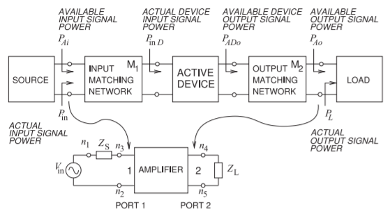
Figure \(\PageIndex{2}\): Parameters used in defining gain measures. The input and output matching networks are lossless so that the actual device input signal power, \(P_{\text{in}D}\), is the power delivered by the source. Similarly the actual output signal power delivered to the load, \(P_{L}\), is the power delivered by the active device (the transistor including biasing network).
| Power | Description |
|---|---|
| \(P_{\text{in}}\) | Actual input power delivered to the amplifier. |
| \(P_{Ai}\) | Available input power from the source. \(P_{\text{in}}\leq P_{Ai}\). If \(\text{M}_{1}\) provides conjugate matching as seen from the source, then \(P_{\text{in}} = P_{Ai}\). |
| \(P_{\text{in}D}\) | Actual device input power delivered to the active device. \(P_{\text{in}D}\leq P_{\text{in}}\). If \(\text{M}_{1}\) is lossless, \(P_{\text{in}D} = P_{\text{in}}\). |
| \(P_{ADo}\) | Available device output power of the active device. |
| \(P_{Ao}\) | Available amplifier output power. \(P_{Ao}\leq P_{ADo}\). If \(\text{M}_{2}\) is lossless, \(P_{Ao} = P_{ADo}\). |
| \(P_{L}\) | Actual output power delivered to load. Amplifier output power. \(P_{L}\leq P_{Ao}\). If \(\text{M}_{2}\) is lossless and provides conjugate matching, \(P_{L} = P_{Ao} = P_{ADo}\). |
Table \(\PageIndex{2}\)
coupled with experience, to formulate an idea of how difficult a design will be.
The quantities used in the various gain definitions are defined in Figure \(\PageIndex{2}\). The power delivered to the amplifier is \(P_{\text{in}}\), and this is equal to the available input power from the source if the source is conjugately matched to the input matching network. The power delivered to the active device, \(P_{\text{in}D}\), is equal to the amplifier input power, \(P_{\text{in}}\), if the input matching network is lossless. The available output power from the active device, \(P_{Ao}\), is the actual device output power, \(P_{o}\), delivered to the output matching network if the output of the active device is conjugately matched. This power is also delivered to the load as \(P_{L}\) if \(\text{M}_{2}\) is lossless. In summary,
\[\begin{array}{ll}{P_{\text{in}}=P_{Ai}}&{\text{if the generator is conjugately matched}}\\{P_{\text{in}}=P_{\text{in}D}}&{\text{if }M_{1}\text{ is the lossless}}\\{P_{o}=P_{Ao}}&{\text{if the output of active device is conjugately matched}}\\{P_{L}=P_{o}}&{\text{if }M_{2}\text{ is lossless}}\end{array}\nonumber \]
These power definitions refer to different circuit conditions. This enables a number of different gain definitions to be developed that relate to different stages in the development of an amplifier and indicate the ultimate performance achievable from an amplifier. The basic gain definitions are
- System gain:
\[\label{eq:1}G=\frac{P_{L}}{P_{\text{in}}} \]
The system gain is the power actually delivered to the load relative to the input power delivered by the source. This gain is sometimes called the actual power gain. - Power gain:
\[\label{eq:2}G_{P}=\frac{P_{L}}{P_{\text{in,}D}} \]
The gain is \(G\), but with the loss of \(M_{1}\) removed. - Transducer gain:
\[\label{eq:3}G_{T}=\frac{P_{L}}{P_{Ai}} \]
This is the ratio of the power delivered to the load divided by the power available from the source. This is the gain that really matters, the power actually delivered to the load relative to the power available from the source. - Available gain:
\[\label{eq:4}G_{A}=\frac{P_{Ao}}{P_{Ai}} \]
The transducer gain is the power available to the load relative to the input power available from the source. This gain is \(G_{T}\) with optimum \(M_{2}\). That is, \(G_{A}\) is the system gain \(G\) with lossless \(M_{1}\) and \(M_{2}\) both optimized for maximum power transfer.
These gains are measures that can be used to characterize the performance of an amplifier but do not guide design. The development of guidelines begins by developing expressions for gains using the device’s \(S\) parameters and then considering gain under idealized conditions such as optimum matching networks or with the device adjusted using feedback so that it is effectively unilateral.
Example \(\PageIndex{1}\): Amplifier Gain
A source that drives an amplifier has an available output power of \(1\text{ mW}\). However, the load of the amplifier is mismatched so that the load reflection coefficient is \(1\text{ dB}\). The power actually delivered to the load of the amplifier is \(1\text{ W}\). Is it possible to determine the system gain? If so, what is it in decibels?
Solution
There are many gain definitions so the information provided must be examined. The power delivered to the load is \(P_{L} = 1\text{ W}\), and the available input power \(P_{Ai} = 1\text{ mW}\). Examining the gains defined in Equations \(\eqref{eq:1}\)–\(\eqref{eq:4}\), Equation \(\eqref{eq:3}\) yields
\[\label{eq:5}G_{T}=\frac{P_{L}}{P_{Ai}}=\frac{1\text{ w}}{1\text{ mW}}=1000=30\text{ dB} \]
No other gain can be determined, i.e., the system gain cannot be determined as the actual input power is unknown.
2.3.1 Gain in Terms of Scattering Parameters
This section develops the generalized scattering parameters of an amplifier and leads to expressions for gain in terms of the \(S\) parameters of the active device.
A linear amplifier can be represented as a two-port with a Thevenin equivalent source at Port \(1\) and a load at Port \(2\), as shown in Figure \(\PageIndex{3}\)(a). This section illustrates the usefulness of generalized \(S\) parameters in working with power flow in systems with different system impedances at the ports. Let \(\mathbf{S}\) be the normalized scattering matrix of the two-port, with \(Z_{0}\) being the normalizing real characteristic impedance:
\[\label{eq:6}\mathbf{S}=[S]=\left[\begin{array}{cc}{S_{11}}&{S_{12}}\\{S_{21}}&{S_{22}}\end{array}\right] \]
The development in this section uses the normalized \(S\) parameters of the amplifier in Figure \(\PageIndex{3}\)(a). The aim is to develop an expression for the
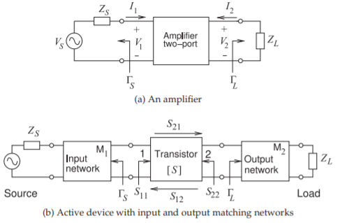
Figure \(\PageIndex{3}\): Two-port network with source and load used in defining unilateral gain measures.
unilateral transducer gain and for the maximum unilateral transducer gain. The unilateral transducer gain is restricted to the amplifier (Figure \(\PageIndex{3}\)(a)), and the maximum unilateral transducer gain can use the \(S\) parameters of either the transistor (Figure \(\PageIndex{3}\)(b)) or the amplifier (Figure \(\PageIndex{3}\)(a)).
The generalized scattering matrix of the amplifier will be normalized to the source impedance, \(Z_{S}\), and load impedance, \(Z_{L}\), shown in Figure \(\PageIndex{3}\). First, the reflection coefficients \(\Gamma_{S}\) and \(\Gamma_{L}\) (normalized to \(Z_{0}\)) at the source and load are found using
\[\label{eq:7}\Gamma_{S}=\frac{Z_{S}-Z_{0}}{Z_{S}+Z_{0}}\quad\text{and}\quad\Gamma_{L}=\frac{Z_{L}-Z_{0}}{Z_{L}+Z_{0}} \]
From Equation (2.132) of [2], the generalized scattering parameters (with Port \(1\) normalized to \(Z_{S}\) and Port \(2\) normalized to \(Z_{L}\)) are
\[\label{eq:8}\:^{G}\mathbf{S}=(\mathbf{D}^{\ast})^{-1}(\mathbf{S}-\mathbf{\Gamma}^{\ast})(\mathbf{U}-\mathbf{\Gamma S})^{-1}\mathbf{D} \]
where
\[\begin{align}\label{eq:9}\Gamma&=\left[\begin{array}{cc}{\Gamma_{S}}&{0}\\{0}&{\Gamma_{L}}\end{array}\right],\quad\mathbf{D}=\left[\begin{array}{cc}{D_{11}}&{0}\\{0}&{D_{22}}\end{array}\right] \\ \label{eq:10}D_{11}&=\frac{(1-\Gamma_{S})\sqrt{1-|\Gamma_{S}|^{2}}}{|1-\Gamma_{S}^{\ast}|}\quad\text{and}\quad D_{22}=\frac{(1-\Gamma_{L})\sqrt{1-|\Gamma_{L}|^{2}}}{|1-\Gamma_{L}^{\ast}|}\end{align} \]
Following tedious algebraic manipulations, the following expressions are obtained:
\[\begin{align}\label{eq:11}\:^{G}S_{11}&=\frac{1}{W}\frac{1-\Gamma_{S}}{1-\Gamma_{S}^{\ast}}[(S_{11}-\Gamma_{S}^{\ast})(1-\Gamma_{L}S_{22})+S_{12}S_{21}\Gamma_{L}] \\ \label{eq:12}\:^{G}S_{12}&=\frac{1}{W}\frac{(1-\Gamma_{S})(1-\Gamma_{L})}{|1-\Gamma_{S}||1-\Gamma_{L}|}S_{12}[(1-|\Gamma_{S}|^{2})(1-|\Gamma_{L}|^{2})]^{\frac{1}{2}} \\ \label{eq:13}\:^{G}S_{21}&=\frac{1}{W}\frac{(1-\Gamma_{S})(1-\Gamma_{L})}{|1-\Gamma_{S}||1-\Gamma_{L}|}S_{21}[(1-|\Gamma_{S}|^{2})(1-|\Gamma_{L}|^{2})]^{\frac{1}{2}} \\ \label{eq:14}\:^{G}S_{22}&=\frac{1}{W}\frac{1-\Gamma_{L}}{1-\Gamma_{L}^{\ast}}[(S_{22}-\Gamma_{L}^{\ast})(1-\Gamma_{S}S_{11})+S_{12}S_{21}\Gamma_{S}] \end{align} \]
where
\[\label{eq:15}W=(1-\Gamma_{S}S_{11})(1-\Gamma_{L}S_{22})-S_{12}S_{21}\Gamma_{S}\Gamma_{L} \]
and
\[\label{eq:16}\left[\begin{array}{c}{b_{1}}\\{b_{2}}\end{array}\right]=\:^{G}\mathbf{S}\left[\begin{array}{c}{a_{1}}\\{a_{2}}\end{array}\right] \]
Here \(a\) and \(b\) are the root power waves defined in Figure 2-17 of [2].
A number of useful observations can be made. First, in a matched condition where \(\Gamma_{S} = \Gamma_{L} = 0\) (i.e., \(Z_{S} = Z_{L} = Z_{0}\)), \(\:^{G}\mathbf{S} = \mathbf{S}\). Second, for a reciprocal two-port network with \(S_{12} = S_{21}\), the generalized scattering parameters are also reciprocal (i.e., \(^{G}S_{12} =\:^{G}S_{21}\)). An amplifier is not reciprocal, however, and for a good amplifier, \(^{G}S_{12}\) is approximately zero and \(|^{G}S_{21}|\) is greater than one, indicating power gain.
Now the transducer power gain, \(G_{T}\), can be expressed in terms of device \(S\) parameters. \(G_{T}\) (Equation \(\eqref{eq:3}\)) is defined as the ratio of the average power, \(P_{L}\), delivered to the load \(Z_{L}\), and the maximum input power available from the generator, \(P_{Ai}\), that is,
\[\label{eq:17}G_{T}=\frac{P_{L}}{P_{Ai}} \]
where the available power from the generator is
\[\label{eq:18}P_{Ai}=\frac{1}{8}\frac{|V_{S}|^{2}}{\Re\{Z_{S}\}}=\frac{1}{2}|a_{1}|^{2} \]
and the power delivered to the load is
\[\label{eq:19}P_{L}=\frac{1}{2}\Re\{Z_{L}\}|-I_{2}|^{2}=\frac{1}{2}|b_{2}|^{2} \]
These quantities are defined in terms of the root power waves \(a_{1}\) and \(b_{2}\) and these are related by the generalized \(S\) parameters. Thus the transducer gain
\[\label{eq:20}G_{T}=\left|\frac{b_{2}}{a_{1}}\right|^{2}=|^{G}S_{21}|^{2} \]
and so, using Equation \(\eqref{eq:13}\),
\[\label{eq:21}G_{T}=|S_{21}|^{2}\frac{(1-|\Gamma_{S}|^{2})(1-|\Gamma_{L}^{2})}{|(1-\Gamma_{S}S_{11})(1-\Gamma_{L}S_{22})-\Gamma_{S}\Gamma_{L}S_{12}S_{21}|^{2}} \]
This combines the inherent voltage gain of the device \((S_{21})\) with the effect of load and source mismatches through \(\Gamma_{L}\) and \(\Gamma_{S}\). This expression simplifies under particular circumstances that will now be considered.
If the source and load impedances are both equal to the system impedance, then the transducer gain becomes
\[\label{eq:22}\left.G_{T}\right|_{Z_{0}}=|S_{21}|^{2} \]
This is the transducer gain without matching networks, so that \(\Gamma_{S} =0= \Gamma_{L}\). This is nearly always much lower than what can be achieved using matching networks. For one, an active device has significant input and output reactances at microwave frequencies that need to be tuned out.
For a unilateral two-port, \(S_{12} = 0\) (and this is a reasonable approximation for many amplifiers, as there is little feedback from the output to the input). Then the transducer gain becomes the unilateral transducer gain, \(G_{TU}\):
\[\label{eq:23}G_{TU}=|S_{21}|^{2}\left(\frac{1-|\Gamma_{S}|^{2}}{|1-\Gamma_{S}S_{11}|^{2}}\right)\left(\frac{1-|\Gamma_{L}|^{2}}{|1-\Gamma_{L}S_{22}|^{2}}\right) \]
This is often referred to as just the unilateral gain.
From the last expression it can be seen that by choosing \(\Gamma_{S} = (S_{11})^{\ast}\) and \(\Gamma_{L} = (S_{22})^{\ast}\) (i.e., the complex conjugates), \(G_{TU}\) achieves its maximum value, the maximum unilateral transducer gain:
\[\label{eq:24}G_{TU\text{max}}=|S_{21}|^{2}\left(\frac{1}{1-|S_{11}|^{2}}\right)\left(\frac{1}{1-|S_{22}|^{2}}\right) \]
| Frequency \((\text{GHz})\) |
\(G_{TU\text{max}}\) \((\text{dB})\) |
|---|---|
| \(0.5\) | \(36.62\) |
| \(1\) | \(31.07\) |
| \(2\) | \(24.88\) |
| \(3\) | \(21.26\) |
| \(4\) | \(18.73\) |
| \(5\) | \(16.00\) |
| \(6\) | \(15.74\) |
| \(7\) | \(14.52\) |
| \(8\) | \(13.26\) |
| \(9\) | \(12.36\) |
| \(10\) | \(12.24\) |
| \(11\) | \(12.07\) |
| \(12\) | \(11.77\) |
| \(13\) | \(11.46\) |
| \(14\) | \(11.25\) |
| \(15\) | \(11.61\) |
| \(16\) | \(11.64\) |
| \(17\) | \(11.11\) |
| \(18\) | \(10.50\) |
| \(19\) | \(8.89\) |
| \(20\) | \(7.91\) |
| \(21\) | \(7.48\) |
| \(22\) | \(6.55\) |
| \(23\) | \(5.46\) |
| \(24\) | \(4.62\) |
| \(25\) | \(4.22\) |
| \(26\) | \(3.61\) |
Table \(\PageIndex{3}\): Maximum unilateral transducer gain, \(G_{TU\text{max}}\), of the pHEMT transistor documented in Table \(\PageIndex{1}\).
Note that up to now the \(S\) parameters have been those of the transistor, see Figure \(\PageIndex{3}\)(b). So \(G_{TU\text{max}}\) is the maximum unilateral transducer gain available from the active device. This is a good measure of the maximum power gain readily obtained from the device. However, with feedback (consider the general amplifier configuration of Figure 2.6.4) the effective \(S_{12}\neq 0\), and any gain can be achieved, even oscillation. Also, higher gain is obtained at the expense of reduced bandwidth. As a general design guideline, the closer the gain specified for an amplifier is to \(G_{TU\text{max}}\), the more challenging the design task.
The maximum unilateral transducer gain, \(G_{TU\text{max}}\), of the pHEMT transistor described in Table \(\PageIndex{1}\) in shown in Table \(\PageIndex{3}\). The maximum unilateral transducer gain is largest at low frequencies and monotonically reduces as frequency increases. This means that it is difficult to design a broadband amplifier using a pHEMT (and this is true with most FETs). It is also a challenge to ensure stable amplification at low frequencies and matching networks must be chosen to suppress low-frequency gain.
The power gain with the input conjugately matched is
\[\label{eq:25}G_{P}=\frac{|S_{21}|^{2}(1-|\Gamma_{L}|^{2})}{|(1-S_{22}\Gamma_{L})(1-|S_{11}|^{2})} \]
and with \(\Gamma_{L} = 0\),
\[\label{eq:26}\left. G_{P}\right|_{\Gamma_{L}=0}=\frac{|S_{21}|^{2}}{(1-|S_{11}|^{2})} \]
The available power gain with the output conjugately matched is
\[\label{eq:27}G_{A}=\frac{|S_{21}|^{2}(1-|\Gamma_{S}|^{2})}{|1-S_{11}\Gamma_{S}|^{2}(1-|S_{22}|^{2})} \]
and with \(\Gamma_{S}=0\),
\[\label{eq:28}\left. G_{A}\right|_{\Gamma_{S}=0}=\frac{|S_{21}|^{2}}{1-|S_{22}|^{2}} \]
The maximum available power gain, \(G_{\text{MA}}\), equal to both \(G_{A}\) and \(G_{T}\) with optimum \(M_{1}\) and \(M_{2}\) is
\[\label{eq:29}G_{\text{MA}}=\left|\frac{S_{21}}{S_{12}}\right|\left(k-\sqrt{k^{2}-1}\right) \]
where the Rollet’s stability factor [3, 4]
\[\label{eq:30}k=\left(\frac{1-|S_{11}|^{2}-|S_{22}|^{2}+|\Delta|^{2}}{2|S_{12}||S_{21}|}\right)\quad\text{and}\quad\Delta =S_{11}S_{22}-S_{12}S_{21} \]
Rollett developed the expressions for \(G_{\text{MA}}\) and \(k\) in terms of \(z,\: y,\) and \(h\) parameters [3, 4]. The expressions in Equations \(\eqref{eq:29}\) and \(\eqref{eq:30}\) are developed using the equivalences given in Table 2-2 of [2].
\(G_{\text{MA}}\) is only defined when \(k\geq 1\) indicating that if \(k < 1\) the amplifier can be expected to oscillate if both \(M_{1}\) and \(M_{2}\) are optimized for maximum power transfer. Provided that \(k\geq 1\), \(G_{\text{MA}}\) is the maximum gain that can be achieved without using feedback from the output of the active device to its input. It is still possible to obtain stable gain when \(k < 1\) but it is necessary to use either nonoptimum \(M_{1}\) or \(M_{2}\), or feedback across the active device.
Another important gain metric is the maximum stable gain \(G_{\text{MS}}\) that can be achieved. Of course this is just \(G_{\text{MA}}\) if the amplifier is unconditionally stable. If \(k < 1\), Rollett showed that the amplifier is potentially unstable (this will be discussed in greater detail in Section 2.6) [3, 4]. Then \(G_{\text{MS}}\) will be less than \(G_{\text{MA}}\). Rollett ensured stability of the amplifier by putting shunt admittances at the input and output ports of the transistor so that for the augmented transistor two-port \(k = 1\). Then the maximum stable power gain, \(G_{\text{MS}}\), is \(G_{\text{MA}}\) in Equation \(\eqref{eq:29}\) but with \(k\) set to \(1\):
\[\label{eq:31}G_{\text{MS}}=\left|\frac{S_{21}}{S_{12}}\right| \]
From Table 2-2 of [2] it is seen that \(S_{21}/S_{12} = z_{21}/z_{12} = y_{21}/y_{12} = h_{21}/h_{12}\) so that the surprising result is that the maximum stable gain, a power gain, is the ratio of the forward parameter to the reverse parameter and not the square of the ratio, and those parameters could be \(S,\: z,\: y,\) or \(h\) parameters.
Experience indicates that \(G_{\text{MS}}\) is the practical limit to the stable gain that can be achieved with moderate design effort. (Note that the amplifier could be stable without being conditionally stable which is the criterion used in developing \(G_{\text{MS}}\), and schemes other than using shunt admittances could be used to achieve unconditional stability). \(G_{\text{MS}}\) is interpreted as the maximum gain that can be achieved while ensuring that the amplifier is unconditionally stable.
The final useful gain metric is the unilateral power gain, \(U\). This is the maximum available gain, \(G_{\text{MA}}\), with feedback across the active device adjusted so that the effective device feedback parameter \(S_{12} = 0\). When \(U = 1\), the devices go from being active to being passive [5]:
\[\label{eq:32}U=\left(\frac{|S_{21}/S_{12}-1|^{2}}{2k|S_{21}/S_{12}|-2\Re (S_{21}/S_{12})}\right) \]
2.3.2 Design Using Gain Metrics
\(G_{TU\text{,max}},\: G_{\text{MS}},\: G_{\text{MA}}\), and \(U\) are used by designers as measures of the ultimate performance of a device and to guide design. They are important FOMs
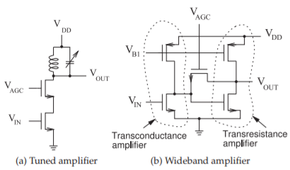
Figure \(\PageIndex{4}\): Low-noise amplifiers. \(V_{\text{AGC}}\) is the automatic gain control voltage and sets the gain of the amplifiers.
as they are defined with extreme conditions. Of these metrics only \(G_{\text{MA}}\) relates to the unaltered device \(S\) parameters. \(G_{\text{MA}}\) is the maximum gain that can be obtained with optimum input and output matching networks. If the amplifier is potentially unstable with optimum \(M_{1}\) and \(M_{2}\), then \(G_{\text{MA}}\) is undefined.
\(G_{TU\text{,max}}\) is the gain when the effective \(S_{12}\) is set to zero (perhaps using feedback) but instead of optimum \(M_{1}\) and \(M_{2}\), \(\Gamma_{S}\) is set to \(S_{11}^{\ast}\) and \(\Gamma_{L}\) is set to \(S_{22}^{\ast}\). (\(S_{11}\) and \(S_{22}\) are those of the active device and are unaffected by feedback.) With \(S_{12} = 0\), the choice for \(\Gamma_{L}\) is the same as using an optimum \(M_{2}\). However the choice for \(\Gamma_{S}\) (i.e. \(\Gamma_{S} = S_{11}^{\ast}\)) is not the same as using an optimum \(M_{1}\). Choosing an optimum \(M_{1}\) would lead to a higher system gain (i.e., \(G>G_{TU\text{,max}}\)). Experience is that \(G_{TU\text{,max}}\) can be achieved with little design effort. It is used primarily in initial choice of the active device.
\(G_{\text{MS}}\) and \(U\) are the maximum available gains for two different specific although artificial conditions. \(G_{\text{MS}}\) is the maximum available gain with \(k\) set \(1\), perhaps using feedback, but otherwise not changing the device’s \(S\) parameters. Design experience is that \(G_{\text{MS}}\) is the stable gain that can be achieved with moderate design effort. \(U\) is the maximum available gain with \(S_{12}\) set to \(1\), perhaps using feedback, but otherwise not changing the device’s \(S\) parameters. The design experience is that \(U\) indicates the highest frequency at which gain can be achieved and this is when \(U = 1\).
\(G_{TU\text{,max}},\: G_{\text{MS}},\: G_{\text{MA}}\), and \(U\) are tabulated in Table \(\PageIndex{4}\) for the pHEMT transistor documented in Table \(\PageIndex{1}\). As will be shown in Section 2.6.3, the amplifier is unconditionally stable from \(5\) to \(11\text{ GHz}\) and above \(22\text{ GHz}\). Outside those ranges, matching networks can be chosen so that the amplifier could oscillate and then \(G_{\text{MA}}\) is not defined. \(G_{\text{MS}}\) is usually taken as the highest gain that can be easily achieved. However, higher gains can be achieved with more attention to stability, but then usually amplification is available only over a very narrow bandwidth.
Once a design is completed, the only gain that matters is the transducer gain, \(G_{T}\), which is the ratio of the power delivered to a load to the power available from the source.
2.3.3 Gain Circles
The expressions for gains developed in Section 2.3.1 were in terms of absolute values of complex numbers. It is therefore possible to present gains at a particular frequency using circles on the complex reflection coefficient
| Freq. \((\text{GHz})\) |
Max. unilateral transducer gain \(G_{TU,\text{max}}\) \((\text{dB})\) |
Max. available power gain \(G_{\text{MA}}\) \((\text{dB})\) |
Max. stable power gain \(G_{\text{MS}}\) \((\text{dB})\) |
Unilateral power gain \(U\) \((\text{dB})\) |
|---|---|---|---|---|
| \(0.5\) | \(36.6\) | \(-\) | \(30.1\) | \(41.9\) |
| \(1\) | \(31.1\) | \(-\) | \(27.1\) | \(39.4\) |
| \(2\) | \(24.9\) | \(-\) | \(24.2\) | \(34.4\) |
| \(3\) | \(21.3\) | \(-\) | \(22.4\) | \(29.7\) |
| \(4\) | \(18.7\) | \(-\) | \(21.3\) | \(25.6\) |
| \(5\) | \(17.0\) | \(18.6\) | \(20.4\) | \(23.6\) |
| \(6\) | \(15.7\) | \(17.0\) | \(19.6\) | \(22.6\) |
| \(7\) | \(14.5\) | \(15.5\) | \(18.7\) | \(20.8\) |
| \(8\) | \(13.6\) | \(14.0\) | \(18.2\) | \(17.9\) |
| \(9\) | \(12.4\) | \(13.0\) | \(17.7\) | \(16.4\) |
| \(10\) | \(12.2\) | \(13.2\) | \(16.6\) | \(17.8\) |
| \(11\) | \(12.1\) | \(13.7\) | \(15.7\) | \(19.5\) |
| \(12\) | \(11.8\) | \(-\) | \(14.8\) | \(20.5\) |
| \(13\) | \(11.5\) | \(-\) | \(14.2\) | \(20.5\) |
| \(14\) | \(11.2\) | \(-\) | \(13.5\) | \(21.2\) |
| \(15\) | \(11.6\) | \(-\) | \(13.1\) | \(27.6\) |
| \(16\) | \(11.6\) | \(-\) | \(12.7\) | \(24.2\) |
| \(17\) | \(11.1\) | \(-\) | \(12.3\) | \(21.4\) |
| \(18\) | \(10.5\) | \(-\) | \(11.9\) | \(17.0\) |
| \(19\) | \(8.88\) | \(-\) | \(11.5\) | \(12.9\) |
| \(20\) | \(7.91\) | \(-\) | \(11.2\) | \(11.4\) |
| \(21\) | \(7.48\) | \(-\) | \(10.9\) | \(11.0\) |
| \(22\) | \(6.55\) | \(8.42\) | \(10.4\) | \(9.22\) |
| \(23\) | \(5.46\) | \(6.62\) | \(9.97\) | \(7.43\) |
| \(24\) | \(4.62\) | \(5.55\) | \(9.62\) | \(6.22\) |
| \(25\) | \(4.23\) | \(5.17\) | \(9.05\) | \(5.73\) |
| \(26\) | \(3.61\) | \(4.27\) | \(8.57\) | \(4.79\) |
Table \(\PageIndex{4}\): Device gain metrics for the pHEMT transistor in Table \(\PageIndex{1}\).
plane [6]. The mathematics behind this are developed in Section 1.A.13 of [7].
Two of the more useful gains to use in making trade-offs are the maximum available gain \(G_{\text{MA}}\) (Equation \(\eqref{eq:29}\)) and the maximum stable gain \(G_{\text{MS}}\) (Equation \(\eqref{eq:31}\)). \(G_{\text{MA}}\) is the available \(G_{A}\) and \(G_{T}\) with optimum \(M_{1}\) and \(M_{2}\), but only has a finite value when the transistor is unconditionally stable. Microwave circuit simulators use another gain measure to handle this situation. If a transistor is conditionally stable then resistive loading is used to ensure unconditional stability. So the maximum available gain calculated in microwave simulators is \(G_{\text{MA}}\) if it has a finite value but is \(G_{\text{MS}}\) otherwise. Introducing \(G_{\text{MAX}}\) to describe this gain:
\[\label{eq:33}G_{\text{MAX}}=\left\{\begin{array}{ll}{G_{\text{MA}}=\left|\frac{S_{21}}{S_{12}}\right|(k-\sqrt{k^{2}-1})}&{\text{if }k\geq 1}\\{G_{\text{MS}}=\left|\frac{S_{21}}{S_{12}}\right|}&{\text{if }k<1}\end{array}\right. \]
Here \(k\) is Rollet’s stability factor (see Equation \(\eqref{eq:30}\).
The discussion can now turn to defining gain circles. Gain circles plot the locus of the available power gain, \(G_{A}\), as defined in Equation \(\eqref{eq:27}\), on the input reflection coefficient, \(\Gamma_{S}\), plane. \(G_{A}\) is a function of the magnitude of complex numbers and so circles can be defined in the complex plane. Figure
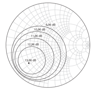
Figure \(\PageIndex{5}\): Gain circles of the transistor in Table \(\PageIndex{1}\) at \(8\text{ GHz}\) plotted on the \(\Gamma_{S}\) plane.
\(\PageIndex{5}\) plots the \(G_{A}\) gain circles for the pHEMT transistor at \(8\text{ GHz}\) on the input reflection coefficient plane. The center of the family of circles is \(G_{\text{MAX}}\) and this point defines the \(\Gamma_{S}\) value required to achieve \(G_{\text{MAX}}\). The other circles moving out plot the locus of \(\Gamma_{S}\) for reductions of available power gain, \(G_{A}\), in \(1\text{ dB}\) steps below \(G_{\text{MAX}}\). That is, a circle defines the values of \(\Gamma_{S}\) that will yield a specific \(G_{A}\).