
4.3: Switching Amplifiers, Classes D, E, and F
- Page ID
- 46064
\( \newcommand{\vecs}[1]{\overset { \scriptstyle \rightharpoonup} {\mathbf{#1}} } \)
\( \newcommand{\vecd}[1]{\overset{-\!-\!\rightharpoonup}{\vphantom{a}\smash {#1}}} \)
\( \newcommand{\dsum}{\displaystyle\sum\limits} \)
\( \newcommand{\dint}{\displaystyle\int\limits} \)
\( \newcommand{\dlim}{\displaystyle\lim\limits} \)
\( \newcommand{\id}{\mathrm{id}}\) \( \newcommand{\Span}{\mathrm{span}}\)
( \newcommand{\kernel}{\mathrm{null}\,}\) \( \newcommand{\range}{\mathrm{range}\,}\)
\( \newcommand{\RealPart}{\mathrm{Re}}\) \( \newcommand{\ImaginaryPart}{\mathrm{Im}}\)
\( \newcommand{\Argument}{\mathrm{Arg}}\) \( \newcommand{\norm}[1]{\| #1 \|}\)
\( \newcommand{\inner}[2]{\langle #1, #2 \rangle}\)
\( \newcommand{\Span}{\mathrm{span}}\)
\( \newcommand{\id}{\mathrm{id}}\)
\( \newcommand{\Span}{\mathrm{span}}\)
\( \newcommand{\kernel}{\mathrm{null}\,}\)
\( \newcommand{\range}{\mathrm{range}\,}\)
\( \newcommand{\RealPart}{\mathrm{Re}}\)
\( \newcommand{\ImaginaryPart}{\mathrm{Im}}\)
\( \newcommand{\Argument}{\mathrm{Arg}}\)
\( \newcommand{\norm}[1]{\| #1 \|}\)
\( \newcommand{\inner}[2]{\langle #1, #2 \rangle}\)
\( \newcommand{\Span}{\mathrm{span}}\) \( \newcommand{\AA}{\unicode[.8,0]{x212B}}\)
\( \newcommand{\vectorA}[1]{\vec{#1}} % arrow\)
\( \newcommand{\vectorAt}[1]{\vec{\text{#1}}} % arrow\)
\( \newcommand{\vectorB}[1]{\overset { \scriptstyle \rightharpoonup} {\mathbf{#1}} } \)
\( \newcommand{\vectorC}[1]{\textbf{#1}} \)
\( \newcommand{\vectorD}[1]{\overrightarrow{#1}} \)
\( \newcommand{\vectorDt}[1]{\overrightarrow{\text{#1}}} \)
\( \newcommand{\vectE}[1]{\overset{-\!-\!\rightharpoonup}{\vphantom{a}\smash{\mathbf {#1}}}} \)
\( \newcommand{\vecs}[1]{\overset { \scriptstyle \rightharpoonup} {\mathbf{#1}} } \)
\( \newcommand{\vecd}[1]{\overset{-\!-\!\rightharpoonup}{\vphantom{a}\smash {#1}}} \)
\(\newcommand{\avec}{\mathbf a}\) \(\newcommand{\bvec}{\mathbf b}\) \(\newcommand{\cvec}{\mathbf c}\) \(\newcommand{\dvec}{\mathbf d}\) \(\newcommand{\dtil}{\widetilde{\mathbf d}}\) \(\newcommand{\evec}{\mathbf e}\) \(\newcommand{\fvec}{\mathbf f}\) \(\newcommand{\nvec}{\mathbf n}\) \(\newcommand{\pvec}{\mathbf p}\) \(\newcommand{\qvec}{\mathbf q}\) \(\newcommand{\svec}{\mathbf s}\) \(\newcommand{\tvec}{\mathbf t}\) \(\newcommand{\uvec}{\mathbf u}\) \(\newcommand{\vvec}{\mathbf v}\) \(\newcommand{\wvec}{\mathbf w}\) \(\newcommand{\xvec}{\mathbf x}\) \(\newcommand{\yvec}{\mathbf y}\) \(\newcommand{\zvec}{\mathbf z}\) \(\newcommand{\rvec}{\mathbf r}\) \(\newcommand{\mvec}{\mathbf m}\) \(\newcommand{\zerovec}{\mathbf 0}\) \(\newcommand{\onevec}{\mathbf 1}\) \(\newcommand{\real}{\mathbb R}\) \(\newcommand{\twovec}[2]{\left[\begin{array}{r}#1 \\ #2 \end{array}\right]}\) \(\newcommand{\ctwovec}[2]{\left[\begin{array}{c}#1 \\ #2 \end{array}\right]}\) \(\newcommand{\threevec}[3]{\left[\begin{array}{r}#1 \\ #2 \\ #3 \end{array}\right]}\) \(\newcommand{\cthreevec}[3]{\left[\begin{array}{c}#1 \\ #2 \\ #3 \end{array}\right]}\) \(\newcommand{\fourvec}[4]{\left[\begin{array}{r}#1 \\ #2 \\ #3 \\ #4 \end{array}\right]}\) \(\newcommand{\cfourvec}[4]{\left[\begin{array}{c}#1 \\ #2 \\ #3 \\ #4 \end{array}\right]}\) \(\newcommand{\fivevec}[5]{\left[\begin{array}{r}#1 \\ #2 \\ #3 \\ #4 \\ #5 \\ \end{array}\right]}\) \(\newcommand{\cfivevec}[5]{\left[\begin{array}{c}#1 \\ #2 \\ #3 \\ #4 \\ #5 \\ \end{array}\right]}\) \(\newcommand{\mattwo}[4]{\left[\begin{array}{rr}#1 \amp #2 \\ #3 \amp #4 \\ \end{array}\right]}\) \(\newcommand{\laspan}[1]{\text{Span}\{#1\}}\) \(\newcommand{\bcal}{\cal B}\) \(\newcommand{\ccal}{\cal C}\) \(\newcommand{\scal}{\cal S}\) \(\newcommand{\wcal}{\cal W}\) \(\newcommand{\ecal}{\cal E}\) \(\newcommand{\coords}[2]{\left\{#1\right\}_{#2}}\) \(\newcommand{\gray}[1]{\color{gray}{#1}}\) \(\newcommand{\lgray}[1]{\color{lightgray}{#1}}\) \(\newcommand{\rank}{\operatorname{rank}}\) \(\newcommand{\row}{\text{Row}}\) \(\newcommand{\col}{\text{Col}}\) \(\renewcommand{\row}{\text{Row}}\) \(\newcommand{\nul}{\text{Nul}}\) \(\newcommand{\var}{\text{Var}}\) \(\newcommand{\corr}{\text{corr}}\) \(\newcommand{\len}[1]{\left|#1\right|}\) \(\newcommand{\bbar}{\overline{\bvec}}\) \(\newcommand{\bhat}{\widehat{\bvec}}\) \(\newcommand{\bperp}{\bvec^\perp}\) \(\newcommand{\xhat}{\widehat{\xvec}}\) \(\newcommand{\vhat}{\widehat{\vvec}}\) \(\newcommand{\uhat}{\widehat{\uvec}}\) \(\newcommand{\what}{\widehat{\wvec}}\) \(\newcommand{\Sighat}{\widehat{\Sigma}}\) \(\newcommand{\lt}{<}\) \(\newcommand{\gt}{>}\) \(\newcommand{\amp}{&}\) \(\definecolor{fillinmathshade}{gray}{0.9}\)Switching amplifiers are the most efficient RF amplifiers, but are also the hardest to design. With linear amplifiers, such as Class A, B, AB, and C amplifiers, there is appreciable simultaneous voltage across the transistor and current flowing through it. Thus power is dissipated in the transistor in such an amplifier. The DC and AC loadlines at the transistor output of a linear amplifier essentially coincide, as is seen in the transistor output characteristic shown in Figure \(\PageIndex{1}\)(a). The DC loadline is a straight line and the AC loadline closely follows the linear DC loadline; this is where the linear in linear amplifier comes from. Even when reactive effects cause the AC loadline to loop (and a small loop is seen in Figure \(\PageIndex{1}\)(a)), the term linear amplifier is still used.
4.3.1 Dynamic Waveforms
In a switching amplifier there is little voltage across the output of the transistor when there is current flowing through it, and little voltage when there is current. This is seen in the AC loadline, also called dynamic loadline, of a switching amplifier, shown in Figure \(\PageIndex{1}\)(b). This loadline is obtained through careful attention to the loading of the transistor at the harmonics.
The dynamic loadline of a switching amplifier is obtained by presenting the appropriate harmonic impedances to the transistor output. The particular scheme of harmonic termination (e.g., short or open circuits at the even and odd harmonics) leads to the designation of a switching amplifier as Classes D, E, F, etc. The key characteristic of all switching amplifiers is that when there is current through the transistor, there is negligible voltage across the output [14, 15, 16, 17, 18, 19, 20]. Also, when there is voltage across the transistor, there is little current through it (see Figure \(\PageIndex{1}\)(b)).
Switching amplifiers are a conceptual departure from Class A, AB, B, and C linear amplifiers. The transistor output waveforms of a switching amplifier and those of Class A, AB, B, and C amplifiers are shown in Figure \(\PageIndex{2}\). Again it is seen, in Figure \(\PageIndex{2}\), that for a switching amplifier the voltages and current waveforms are shifted and voltage across the transistor and current through it do not occur simultaneously. The power dissipated by the transistor is the average of the product of the current through it and the voltage across the output. Thus the ideal switching amplifier consumes very little DC power, transferring nearly all of the DC power to the output RF signal. Bandpass filtering of the output of the amplifier results in a final RF output with little distortion. Switching amplifiers are the preferred amplifier in both handsets and basestations of cellular systems.
The theoretical maximum power-added efficiencies achieved by the various amplifier classes with a sinusoidal input signal are given in Table \(\PageIndex{1}\). With modulated signals, the maximum efficiencies cannot be achieved, as typically the average input power of the amplifier must be backed off by the peak-to-mean envelope power ratio (PMEPR) of the signal so that the peak carrier portion of the signal has limited distortion. Generally the acceptable distortion of the peak signal occurs at the \(1\text{ dB}\) compression point of the amplifier. This is only an approximate guide, but useful. The PMEPRs of several digitally modulated signals are given in Table \(\PageIndex{2}\), together with their impact on efficiency. If there are two carriers, then the PMEPR of the
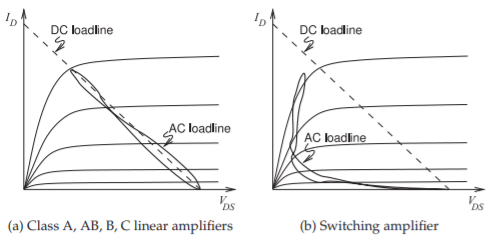
Figure \(\PageIndex{1}\): DC and RF loadlines. An AC loadline is also called a dynamic loadline.
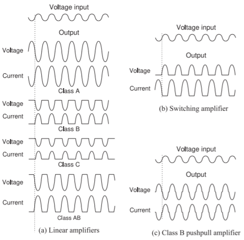
Figure \(\PageIndex{2}\): Input and output waveforms of a transistor for various classes of amplifier. The output voltage is measured across the transistor(s) and the current is through the transistor(s).
| Amplifier Class | Maximum Efficiency |
|---|---|
| Class A (resistive bias) | \(25\%\) |
| Class A (inductive bias) | \(50\%\) |
| Class B | \(78.53\%\) |
| Class C | \(100\%\) |
| Class D | \(100\%\), but typically \(75\%\) |
| Class E | \(96\%\) |
| Class F | \(88.36\%\) |
Table \(\PageIndex{1}\): Theoretical maximum efficiencies of amplifier classes with a sinusoidal excitation.
combined signal will be higher, requiring even greater amplifier backoff [21]. In practice, the efficiencies achieved will differ from these theoretical values. This is because the PMEPR does not fully capture the statistical nature of signals and because of coding and other technologies that can be used to reduce the PMEPR of a digital modulation scheme.
4.3.2 Conduction Angle
The conduction angle indicates the proportion of time an amplifying device, typically a transistor, is conducting current with a conduction angle of \(360^{\circ}\) indicating that the amplifying device is always on. The view is that a sinusoidal signal is being amplified which is appropriate since the majority of communication schemes produce an RF signal that looks like a sinewave with a very slowly-varying amplitude and phase. Class A amplifiers conduct current throughout the RF cycle and so have a conduction angle of \(360^{\circ}\). A Class B amplifier is biased so that only half of a sinewave is produced at the
| Signal | PMEPR \((\text{dB}\)) |
Efficiency Reduction Factor | Class A (L bias) PAE |
Class E PAE |
|---|---|---|---|---|
| FSK (ideal) | \(0\) | \(1.0\) | \(50\%\) | \(96\%\) |
| GMSK | \(3.0\) | \(0.501\) | \(25.1\%\) | \(48.1\%\) |
| QPSK | \(3.6\) | \(0.437\) | \(21.9\%\) | \(42\%\) |
| \(\pi /4\)DQPSK | \(3.0\) | \(0.501\) | \(25.1\%\) | \(48.1\%\) |
| OQPSK | \(3.3\) | \(0.467\) | \(23.4\%\) | \(44.8\%\) |
| \(8\)-PSK | \(3.3\) | \(0.467\) | \(23.4\%\) | \(44.8\%\) |
| \(64\)-QAM | \(7.8\) | \(0.166\) | \(8.3\%\) | \(15.9\%\) |
Table \(\PageIndex{2}\): Efficiency reductions due to modulation type for a single modulated carrier. The Class A amplifier uses inductive drain biasing. The PMEPR increase is for multiple carriers. E.g. for GMSK PMEPR \(= 3.01\text{ dB}\), \(6.02\text{ dB}\), \(9.01\text{ dB}\), \(11.40\text{ dB}\), \(14.26\text{ dB}\), and \(17.39\text{ dB}\) for \(1,\: 2,\: 4,\: 8,\: 16,\) and \(32\) carriers respectively. The PMEPR does not increase by \(3\text{ dB}\) every time the number of carriers is doubled because statistically the envelope peaks of the individual carriers are less likely to align for more carriers.
output, so a Class B amplifier has a conduction angle is \(180^{\circ}\). A Class AB amplifier has a conduction angle between \(180^{\circ}\) and \(360^{\circ}\) with the bias, or one could say conduction angle, adjusted so that the distortion produced is acceptable. A Class C amplifier produces an output for less than half of the input sinewave and so it has a conduction angle of less than \(180^{\circ}\).
Switching amplifiers have high efficiency by ensuring that there is little current flowing through a transistor when there is voltage across it. So a switching amplifier is ideally either fully on or fully off. Ideally current flows for half the time and so the conduction angle is \(180^{\circ}\). However, the transistor must transition between these regions and the conduction angle indicates the degree of overlap. To minimize overlap, the conduction angle of an actual switching amplifier is less than \(180^{\circ}\).
4.3.3 Class D
The Class D amplifier was the first type of switching amplifier developed. The main concept of the Class D amplifier is using the transistor as a switch so that there is negligible current flowing through the transistor when there is voltage across it. The audio form of the Class D amplifier is shown in Figure \(\PageIndex{3}\)(a) [14]. The two transistor inputs have the same RF signal applied but are level-shifted (but the circuit to do this has been omitted as well as the appropriate bias circuitry). Each transistor approximates Class C operation so only one transistor is switched on at a time. The current and voltage waveforms are shown in Figure \(\PageIndex{3}\)(c). The transistors drive a resonant circuit with \(L_{1}\) and \(C_{1}\) acting as a bandpass filter. The filter reduces the distortion of the voltage and current waveforms presented to the output load, but results in the amplifier being narrowband. This Class D amplifier works very well at frequencies up to a few megahertz. Above that the transistors, having opposite polarity, are not well matched. At RF a more appropriate Class D amplifier is as shown in Figure \(\PageIndex{3}\)(b) [14, 15, 19, 22] where, in this case, two nMOS transistors are used as they have higher mobility than pMOS transistors. Parasitic reactances result in substantial overlap of the current and voltage transition regions and hence there is loss of RF power in the
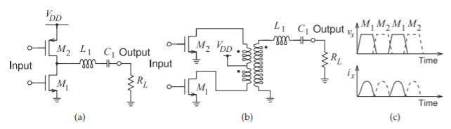
Figure \(\PageIndex{3}\): Class D amplifier: (a) low-frequency form; (b) microwave form; and (c) current and voltage waveforms (where \(v_{x}\) is the drain-source voltage and \(i_{x}\) is the drain current) indicating which transistor is turned on.
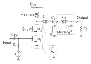
Figure \(\PageIndex{4}\): Class E amplifier.
transistors. This loss can be reduced using an alternative form of the Class D amplifier, called a current-mode Class D amplifier, which switches current rather than voltage [23]. Efficiencies of around \(75\%\) are achieved.
4.3.4 Class E
The Class E [15, 17] amplifier builds on the Class D amplifier concept of using a transistor as a switch rather than as a linear amplifier. An RF Class E amplifier is shown in Figure \(\PageIndex{4}\). The circuit shown uses two MOSFETS with \(M_{1}\) being the switching transistor and \(M_{2}\) acting in part as an active load. The main function of \(M_{2}\) is to translate the drain current of \(M_{1}\) into a voltage at the output. Bias is provided through \(L_{\text{CHOKE}}\), which presents a high RF impedance. \(L_{1}\) and \(C_{1}\) provide a bandpass filtering function, while \(L_{2}\) and \(C_{2}\) provide matching to the load so that the impedance looking into the \(L_{2}\), \(C_{2}\) and \(R_{L}\) network is an optimum resistance, \(R_{\text{opt}}\). The circuit is designed so that \(L_{\text{CHOKE}}\), the parasitic output capacitance of the transistors, \(L_{1}\), \(C_{1}\), and \(R_{\text{opt}}\) form a damped oscillating circuit. The two MOSFETs can also be replaced by a single transistor, typically an HBT transistor, as shown by the insert in Figure \(\PageIndex{4}\), and sometimes a capacitor is added from the top of the transistor to ground if the parasitic transistor capacitance is insufficient. So at the output of the transistors there is a parallel \(LC\) circuit to ground
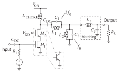
Figure \(\PageIndex{5}\): Class F amplifier.
(\(L_{\text{CHOKE}}\) and the parasitic capacitance of \(M_{2}\)) and a series \(LC\) circuit (\(L_{1}\) and \(C_{1}\)). When the transistors are switched off (and have a high voltage across them), the series \(LC\) circuit provides current to the parallel \(LC\) circuit as well as to \(R_{\text{opt}}\), instead of current being drawn through the transistors. When the transistors are switched on (and have little voltage across them), the oscillation proceeds in the opposite direction and current is delivered to \(R_{\text{opt}}\) through the transistors. This is the oscillation mechanism with the resistance \(R_{\text{opt}}\) providing damping. Design matches the natural oscillation frequency with the frequency of the RF signal.
4.3.5 Class F
In the Class E amplifier the voltage at the drain/collector of the transistor is approximately a square wave and the transistor current approximates a half sinusoid. The Class F amplifier takes this one step further and realizes an approximate square current wave through the transistors as well as an out-of-phase square voltage wave [14, 15, 19]. This is achieved using harmonic resonance.
A Class F amplifier is shown in Figure \(\PageIndex{5}\), where the narrowband RF signal has a center frequency \(f_{0}\). Again \(M_{1}\) operates as a switch producing a square voltage wave at the output of the transistors. The parallel \(L_{1}C_{1}\) circuit is tuned to the third harmonic of the RF signal (i.e., \(3f_{0}\)), and this parallel circuit provides third-harmonic current when the transistors are turned off. The \(L_{1}C_{1}\) circuit is an approximate short circuit at \(f_{0}\), and the parallel \(L_{2}C_{2}\) circuit, tuned to be resonant at \(f_{0}\), presents an open circuit at \(f_{0}\) and short circuits at the harmonics. The net result is that the current waveform passing through the transistors is a reasonable square wave with first and third harmonics and no second harmonic (note that a square wave consists of only odd frequency components). Also note that third-harmonic current does not pass through the load. This concept could be continued to provide similar behavior at the fifth harmonic as well, but it then becomes increasingly difficult to adjust the design to work as intended. With both the voltage and current waves being square, the lower the overlap, and the lower the power dissipated in the transistors.
4.3.6 Inverted Amplifiers
The Class D and F switching amplifiers described above are designed to switch the voltage between two states. The dual of these are the inverted Class D amplifier [20, 23, 24, 25] and the inverted Class F amplifier [26, 27, 28, 29]. The design intent is that the transistors in these amplifiers switch the current rather than the voltage. They are also called current-mode amplifiers.
4.3.7 Summary
The efficiency advantages of switching amplifiers are significant and often justifies the higher design cost. They are used in power amplifiers in most basestations and are starting to be used in cellphones. At high microwave and millimeter-wave frequencies stability concerns and the high cost of design means that many amplifiers will continue to be linear amplifiers for some time.