
11.6: APPLICATIONS INVOLVING ANALOG-SIGNAL SWITCHING
- Page ID
- 75239

Systems that combine operational amplifiers with analog switches add a powerful dimension to the data-processing capability of the amplifiers alone. The switches are often used to control analog operations with digital command signals, and the resultant hybrid (analog-digital) circuits such as analog-to-digital converters are used in a myriad of applications. While a detailed discussion of these advanced techniques is beyond the scope of this book, several simple examples of connections including analog switching are presented in this section.
Either junction-gate or Mos field-effect transistors are frequently used for low-level signal switching. One advantage of a field-effect transistor as an analog switch is that it has no inherent offset voltage. The drain-to-source characteristics of a FET in the on state are linear and resistive for small channel currents, and the drain-to-source voltage is zero for zero channel current. A second advantage is that the channel leakage current of a pinched-off FET is generally under \(1\ nA\) at room temperature. This level is insignificant in many operational-amplifier connections.
There are several integrated circuits available that combine FET'S with drive circuitry to interface the switch to digital-signal levels. Alternatively, discrete-component circuits can be designed to take advantage of the lower on-state resistances generally available from discrete field-effect transistors.
A second possibility is to use a bipolar transistor as a switch. The current handling capacity of bipolar devices is generally higher than that of FET's. However, there is a collector-to-base offset voltage that can be as
high as several hundred millivolts.(One way to reduce the offset voltage of a bipolar transistor is to use it in an inverted or reverse mode with the roles of the emitter and collector interchanged, and offset voltages of a fraction of a millivolt are possible in this connection. The reason for the lower offset in the inverted mode is that the collector-to-emitter voltage of a saturated transistor is, in the absence of ohmic drops, \[V_{\text{offset}} = \dfrac{kT}{q} \ln \dfrac{1}{\alpha}\nonumber \] The reverse common-base current gain \(\alpha_R\) is used to determine forward-region offset, while the forward gain \(\alpha_F\) is used to determine inverted offset voltage. Since \(\alpha_F\) is generally close to one, inverted offset voltages can be quite small. Unfortunately, current gain and breakdown voltages are usually limited in the inverted connection. Consequently, as FET characteristics have improved, these devices have largely replaced inverted bipolar transistors as low-level switches.) Some high-current switching techniques arrange the feedback to eliminate offset-voltage effects.
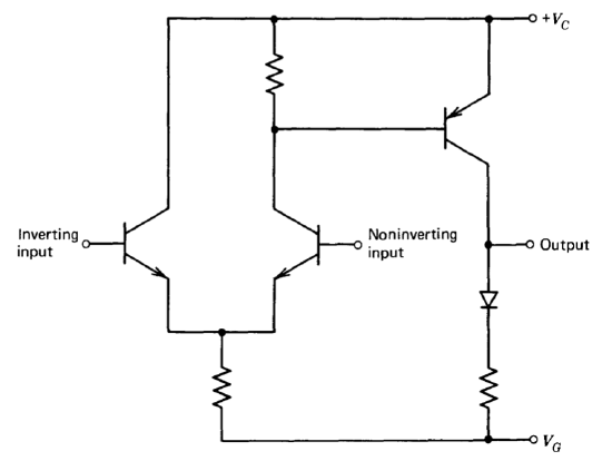
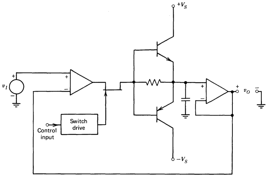
A third type of switch combines the switching and amplification functions in a single circuit. Figure 11.30 shows a possible connection. With \(V_G\) negative, the amplifier is an example of the simple two-stage topology described in Section 8.2.3. If voltage \(V_G\) is switched to a positive potential, all three transistors and the diode become reverse biased, and thus both inputs and the output are open circuits. The gating feature can be retained in designs that expand the simple configuration shown in Figure 11.30 into a complete operational amplifier. Several integrated-circuit examples of this type of design exist (see Section 10.4.2).
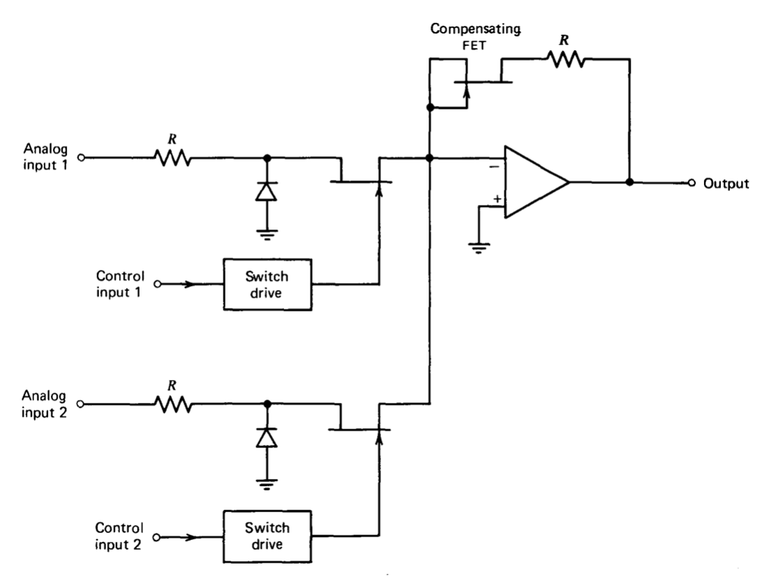
One frequent use for analog switching is to multiplex a number of signals. The required circuit can be realized by using field-effect transistors to switch the signal applied to the input of a noninverting buffer amplifier. Another topology (see Figure 11.31) results in an inverting multiplexer. The advantage of this configuration is that the drive circuit can be simpler than is the case with the noninverting connection. Recall that for a junction FET, it is necessary to make the gate potential approximately equal to the channel potential to turn on the transistor. If the noninverting connection is used, the channel of the on FET will be at the potential of the selected input. Furthermore, one end of the channel of all other switches will also be at the potential of the selected input. These uncertain levels complicate the drive-circuit requirements.
In the inverting topology, the channel of the on FET will be close to ground, and the diodes shown in Figure 11.31 insure that the drain of the off FET will not be significantly more negative than ground. Thus a switch is turned on by grounding its gate, and turned off by making its gate more negative than the pinchoff voltage. An example of a common-base level shifter that converts \(T^2L\) logic signals to the required gate-drive levels is described in Section 12.3.3.
The compensating FET is selected to have an on resistance matched to that of the switches. This device keeps the gain of the multiplexer equal to -1 as on resistance changes with temperature.
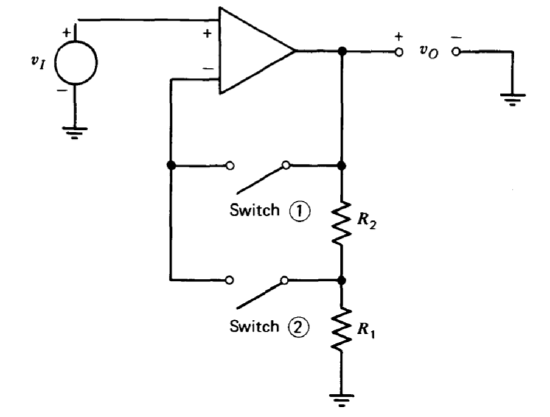
There are a variety of applications that require an amplifier with a selectable closed-loop gain. One topology for this type of gain-range amplifier is shown in Figure 11.32. With switch ① closed and switch ② open, the ideal closed-loop gain is one, while reversing the state of the two switches changes the ideal gain to \((R_1 + R_2)/R_1\). The on resistance of the switches is relatively unimportant because only the low input current of the operational amplifier flows through a switch in this connection.
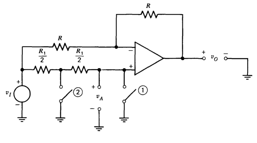
A related circuit function is that of an amplifier that provides a select able gain of plus or minus one. One use for this kind of circuit is in square-wave modulators or demodulators. Figure 11.33 illustrates a possible connection. Assume initially the switch ② is not included in the circuit. With switch ① closed, the amplifier provides an ideal closed-loop gain of -1. With switch ① open, the voltage \(v_A = v_I\), and thus the circuit provides an ideal gain of +1.
Switch ② may be included to reduce the effects of switch on-state resistance. Assume, for example, that design considerations dictate a value for \(R_1\) equal to \(10^3\) times the on-state resistance of a switch. If only switch ① is used, a closed-loop gain error of 0.2% results from this resistance with the switch closed. If both switches are included and closed, the voltage \(v_A\) is reduced by a factor of \(2.5 \times 10^5\) relative to \(v_I\) because of the resulting two stages of attenuation. This attenuation lowers the error from feedthrough to an insignificant level.
There are a number of topologies that combine operational amplifiers with switches to form a sample-and-hold circuit. Figure 11.34 shows one possibility. When the FET conducts, the loop drives the voltage \(v_O\) toward the value of \(v_I\). The complementary emitter-follower pair amplifies the limited current available from the operational amplifier and FET combination so that large currents can be supplied to the capacitor to charge it rapidly. The resistive path between bases and emitters of the follower pair eliminates the deadzone, which would result near equilibrium if the transistors alone were used. While the gain of the first operational amplifier insures that such a deadzone would not influence static characteristics, it could deteriorate stability.
When the switch opens, current into the capacitor is limited to buffer-amplifier input current and switch and emitter-follower leakage current. The base-to-emitter resistor prevents amplification of leakage currents in this state. Since the total capacitor current in the hold mode can be kept small, the held voltage maintains the desired value for prolonged periods.
Note that a field-effect transistor could be used as a buffer as was done in the peak detector described in Section 11.5.2 since the high open-loop gain of the first amplifier would drive the capacitor voltage to the value necessary to make \(v_O = v_I\). However, the output resistance is higher in the hold mode if the FET buffer is used, since feedback is not available to reduce output impedance in the hold mode.
PROBLEMS
Exercise \(\PageIndex{1}\)
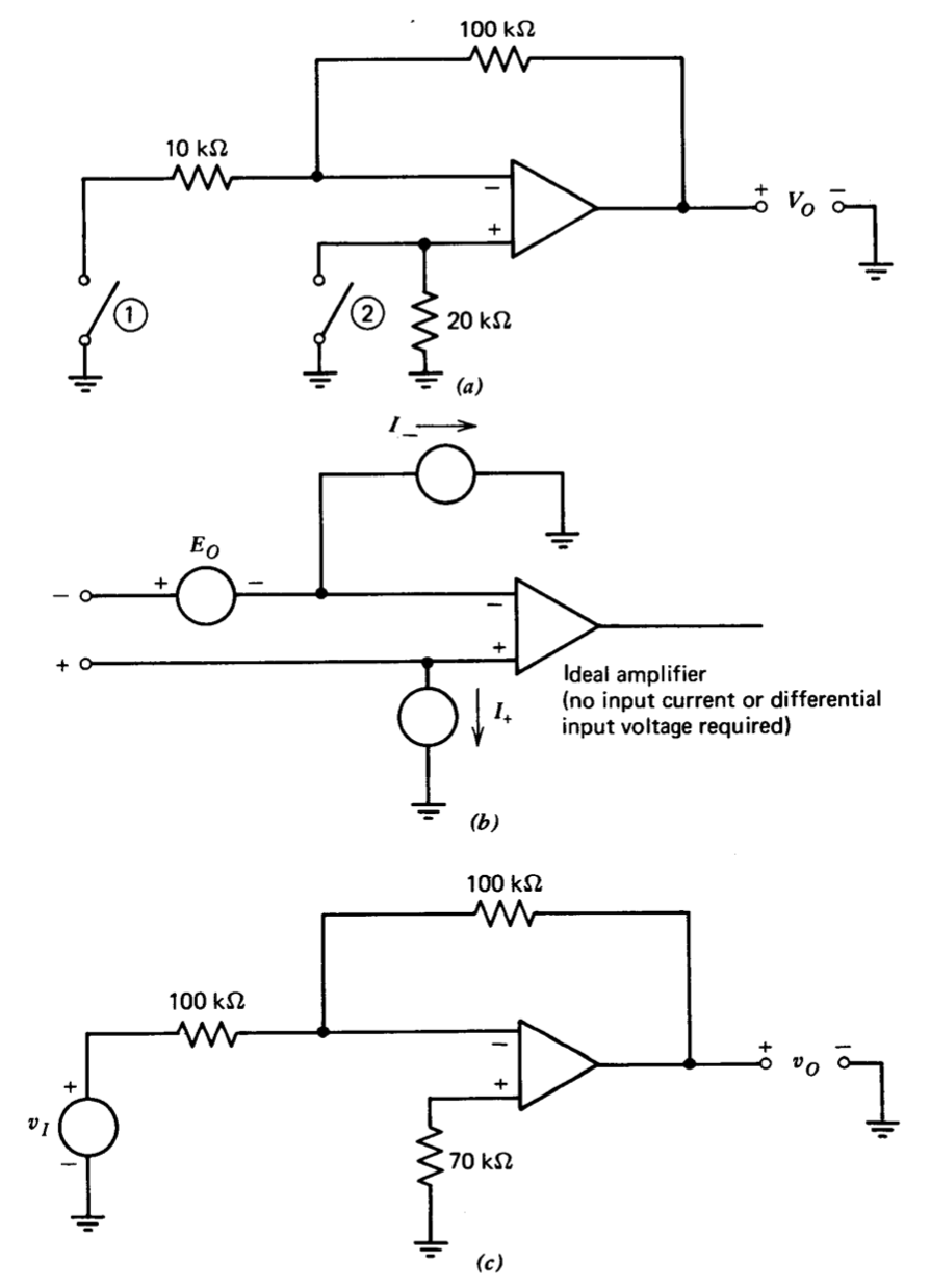
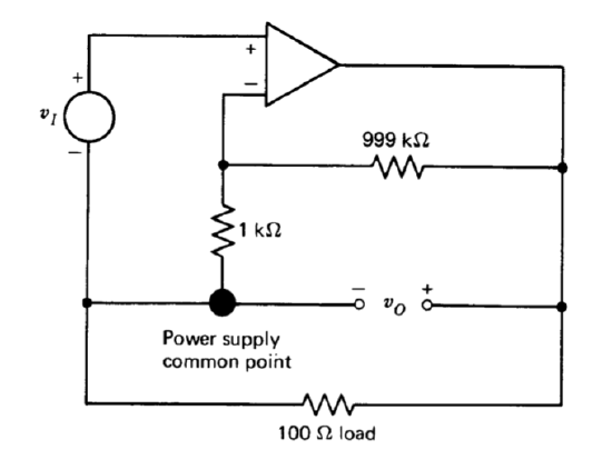
The following results are obtained for measurements made using the circuit shown in Figure 11.35\(a\).
- With switch ① open and switch ② closed, \(V_O = 12\ mV\).
- With switch ① closed and switch ② closed, \(V_O = 32\ mV\).
- With switch ① closed and switch ② open, \(V_O = 10\ mV\).
Determine values for the three bias generators shown in Figure 11.35\(b\). In this representation, the external generators model all bias voltage and cur rent effects so that the input currents and differential input voltage at the terminals of the amplifier shown in the model are zero.
The amplifier is connected as shown in Figure 11.35\(c\). Express \(v_O\) in terms of \(v_I\) and the amplifier parameters shown in Figure 11.35\(b\).
Exercise \(\PageIndex{2}\)
The circuit shown in Figure 11.2\(a\) is used to measure the input offset voltage of an operational amplifier with a d-c open-loop voltage gain of \(10^4\). What error does limited loop transmission introduce into the offset measurement for these parameter values?
Exercise \(\PageIndex{3}\)
A certain operational amplifier is specified to have a maximum input offset voltage magnitude of \(5\ mV\). The amplifier is connected as a unity-gain inverter using two \(2-M\Omega\) resistors. The noninverting input is connected directly to ground. Measurements reveal that the output voltage is \(+50\ mV\) with zero input voltage in this connection. The amplifier in question has provision for reducing the input offset voltage at one temperature to zero by use of an appropriately connected external potentiometer that effectively changes the magnitude of current sources that load the amplifier input-stage transistors. It is found that by use of an extreme setting of the balance pot it is possible to make the output voltage of the inverter zero for zero input voltage. Discuss possible disadvantages of this method of adjustment. Suggest alternatives likely to yield superior performance.
Exercise \(\PageIndex{4}\)
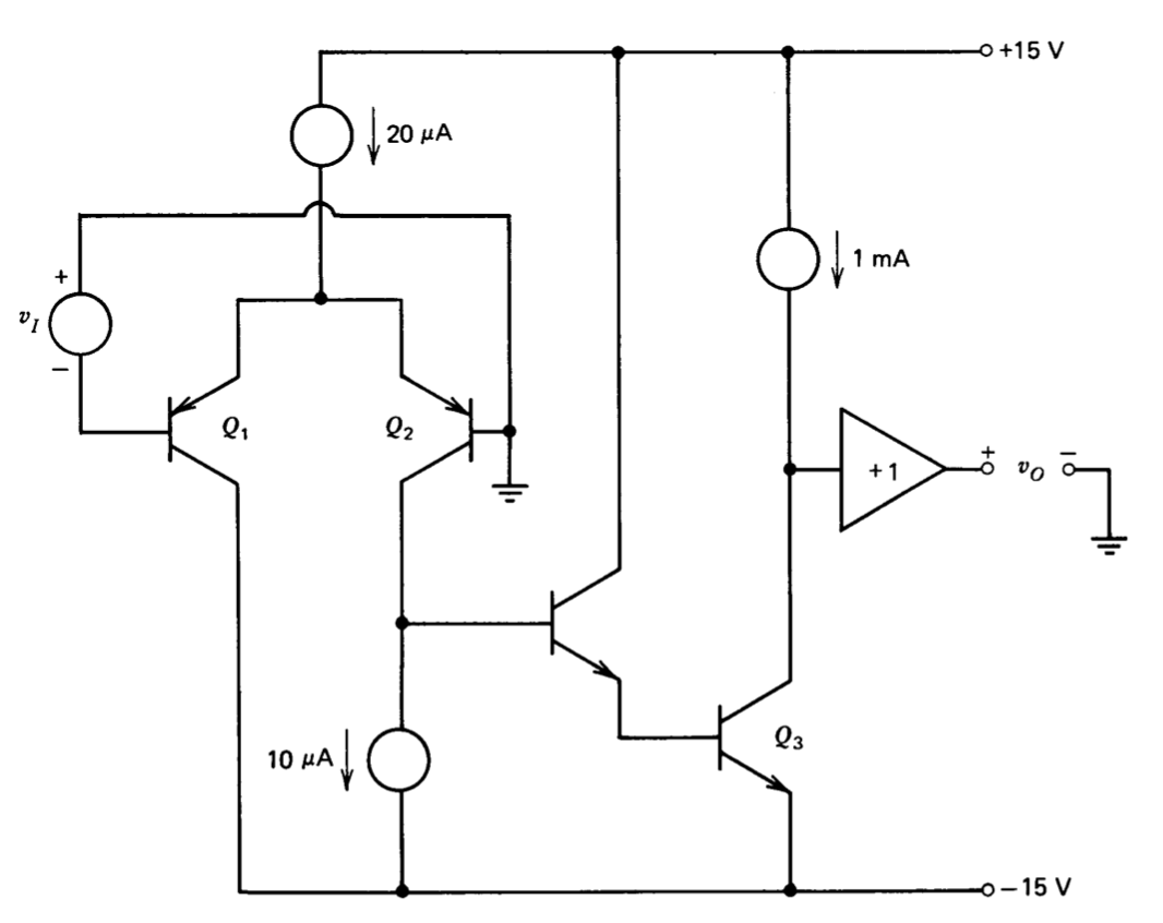
A simplified schematic for an integrated-circuit operational amplifier is shown in Figure 11.36. Careful open-loop gain measurements indicate a gain of 300,000 at 1kHz for the uncompensated amplifier and that the first pole in the amplifier transfer function is above this frequency. In the absence of load, the heating attributable to transistor \(Q_3\) and its current-source load raise the temperature of \(Q_2\ 0.1^{\circ} C\) above that of \(Q_1\) under static conditions with the output at its negative saturation level of -13 volts. Similarly, with the output at its positive saturation level (+ 13 volts) the temperature of transistor \(Q_1\) is eventually raised \(0.1^{\circ} C\) above that of \(Q_2\). Plot the \(v_O\) versus \(v_I\) characteristics that result for very slow variations in \(v_I\). Now assume that the chip locations of transistors \(Q_1\) and \(Q_2\) are interchanged. Again plot the \(v_O\) versus \(v_I\) characteristics. Discuss how these results can complicate measurements of low-frequency open-loop gain.
Exercise \(\PageIndex{5}\)
Integrated-circuit operational amplifiers that use an input stage similar to that of the LM101A (see Section 10.4.1) generally have a high maximum differential input voltage rating. Explain why differential input voltages of approximately 30 volts are possible with this stage compared with the 6-volt maximum level typically specified for a conventional differential amplifier.
Exercise \(\PageIndex{6}\)
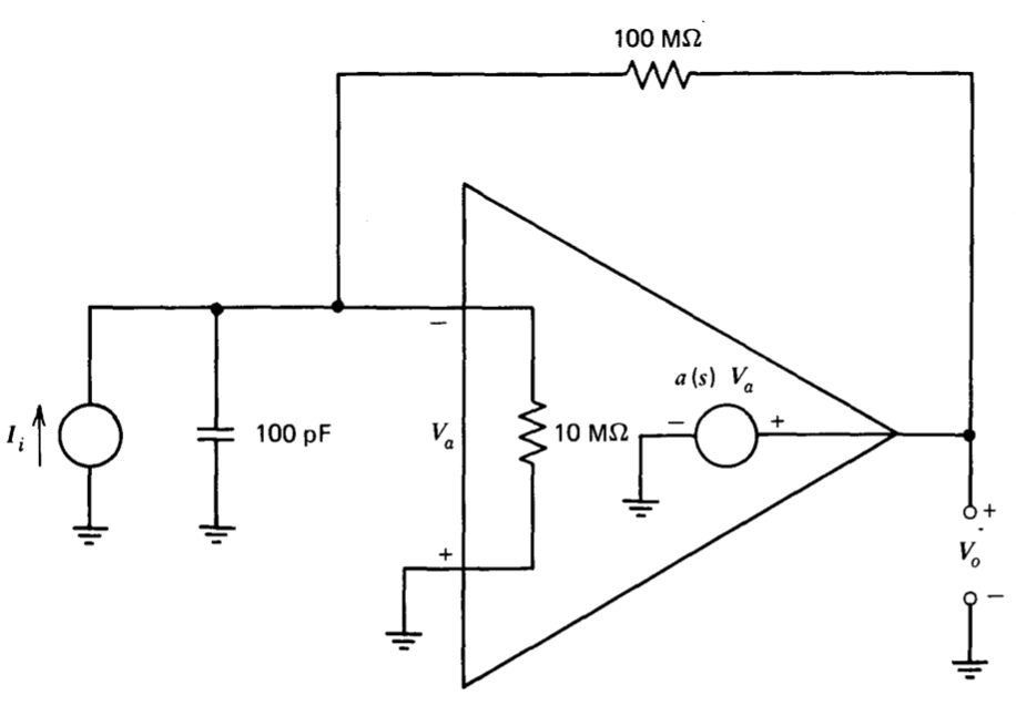
A low input current operational amplifier has an open-loop transfer function
\[a(s) = \dfrac{10^6}{(s + 1)(10^{-5} s + 1)}\nonumber \]
This amplifier is connected to monitor the output current from an ionization gauge. The resultant circuit can be modeled as shown in Figure 11.37. The capacitance shown at the input of the amplifier includes, in addition to the capacitance of the amplifier itself, the capacitance of the gauge and of the shielded cable used to connect the gauge to the amplifier. Investigate the stability of this circuit. Suggest a method for improving stability.
Exercise \(\PageIndex{7}\)
An operational amplifier with high d-c open loop gain and \(100-mA\) output current capacity is connected as shown in Figure 11.38. Low-frequency measurements indicate an incremental gain \(v_o/v_i = 1100\). Explain.
Exercise \(\PageIndex{8}\)
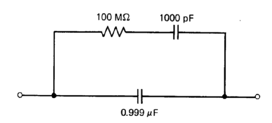
Measurements reveal that the dielectric absorption associated with a certain \(1-\mu F\) capacitor can be modeled as shown in Figure 11.39. Design a circuit that combines this capacitor with an ideal operational amplifier and any necessary passive components such that the closed-loop transfer function is \(-1/s\).
Exercise \(\PageIndex{9}\)
A differential connection as shown in Figure 11.10 is constructed with \(Z_1 = Z_3 = 1\ k\Omega\) and \(Z_2 = Z_4 = 10\ k\Omega\). The operational amplifier has very high d-c open-loop gain and a common-mode rejection ratio of \(10^4\). Assuming all other operational-amplifier characteristics are ideal, what output voltage results with both inputs equal to one volt? Suggest a modification that raises the common-mode rejection ratio for the connection.
Exercise \(\PageIndex{10}\)
An operational amplifier with a d-c open-loop gain of \(10^5\) is connected as a current source with the topology shown in Figure 11.14. The resistor value is \(R = 10\ k\Omega\). With an input voltage of +5 volts, FET parameters are \(y_{fs} = 1\text{ mmho}\) and \(y_{os} = 5 \ \mu \text{mho}\). (See Figure 8.19 for a definition of terms.) What is the incremental output resistance of this connection?
Exercise \(\PageIndex{11}\)
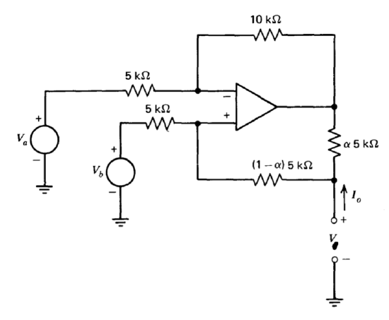
A Howland current source is constructed as shown in Figure 11.40. Determine the current \(I_o\) as a function of \(V_a, V_b, V_o\), and \(\alpha\). Assume that the offset voltage referred to the input of the amplifier is \(5\ mV\) and that the operational amplifier saturates at an output voltage level of \(\pm 10\) volts. Select the parameter a to maximize the output current available at zero output voltage subject to the constraint that \(|i_O| < 5\ \mu A\) with \(v_A = v_B = 0\).
Exercise \(\PageIndex{12}\)
Design a circuit using no inductors that provides a driving-point im pedance \(Z = -1\ k\Omega + 10^{-2}s\).
Exercise \(\PageIndex{13}\)
A nonlinear lag network is required to compensate a servomechanism.(See Section 6.3.5 for a discussion of this type of network.) The network should have a transfer function
\[\dfrac{V_o(s)}{V_i (s)} = \dfrac{0.02s + 1}{s + 1}\nonumber \]
for small input-signal levels. When the magnitude of the voltage across the capacitor exceeds 0.1 volt, the capacitor voltage should be clamped to prevent further increases. Thus the large-signal transfer characteristics will approach \(v_O/v_I \simeq 0.02\), independent of frequency.
Design the required network using a capacitor no larger than \(5\ \mu F\). Provide buffering so that a power amplifier with \(1-k\Omega\) input resistance does not load the network appreciably. The capacitor-voltage limiting level for your design should be relatively temperature independent.
Exercise \(\PageIndex{14}\)
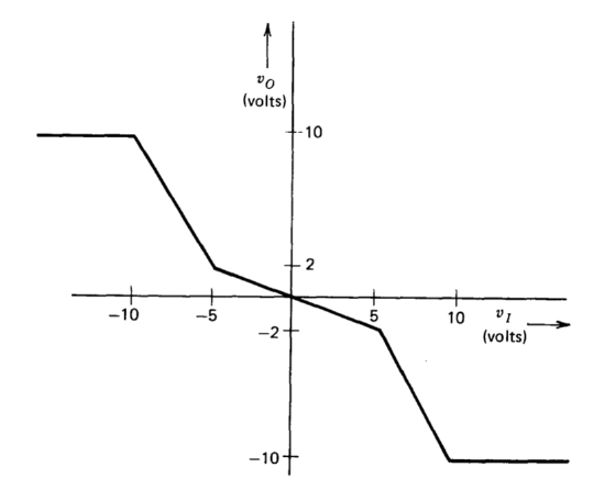
Design a circuit that provides the transfer characteristics shown in Figure 11.41. Use a configuration that makes the breakpoint locations well defined and relatively temperature independent. Select resistor values so that operational-amplifier input bias currents of \(100\ nA\) do not significantly affect performance and so that the loads applied to the outputs of the amplifiers used are less the \(1\ mA\) for any \(|v_I| < 15\text{ volts}\).
Exercise \(\PageIndex{15}\)
Design a circuit that provides an output
\[v_O = \dfrac{\sqrt{v_X v_Y^3}}{10 \text{ volts}} \nonumber \]
You may assume that both \(v_X\) and \(v_Y\) are limited to a range of 0 to \(-10\text{ volts}\). Assume that any operational amplifiers used can provide undistorted outputs of \(\pm 10\text{ volts}\). You should design your circuit so that various voltage levels are close to maximum values for maximum input signal levels in order to improve dynamic range. Comment on the temperature stability of your design.
Exercise \(\PageIndex{16}\)
A sample-and-hold circuit is built using the topology shown in Figure 11.34. The open-loop transfer function of the first operational amplifier is
\[a(s) = \dfrac{10^5}{(0.01s + 1)(5 \times 10^{-8} s + 1)^2}\nonumber \]
and an LM 110 amplifier with a closed-loop bandwidth in excess of 20 MHz is used as the output buffer. The sum of the FET on resistance and the resistor shunting the current-booster transistors is \(1\ k\Omega\), and the capacitor value is \(1\ \mu F\). Investigate the stability of this system under small-signal conditions of operation. Suggest a circuit modification that can be used to improve stability. Comment on the effectiveness of your method under large-signal conditions (with the booster transistors conducting) as well as for linear-region operation.