
13.2: COMPENSATION WHEN THE OPERATIONAL AMPLIFIER TRANSFER FUNCTION IS FIXED
- Page ID
- 58482

Many available operational amplifiers have open-loop transfer functions that cannot be altered by the user. This inflexibility is the general rule in the case of discrete-component amplifiers, and many integrated-circuit designs also include internal (and thus fixed) compensating networks. If the manufacturers’ choice of open-loop transfer function is acceptable in the intended application, these amplifiers are straightforward to use. Conversely, if loop dynamics must be modified for acceptable performance, the choices available to the designer are relatively limited. This section indicates some of the possibilities.
Input Compensation
Input compensation consists of shunting a passive network between the input terminals of an operational amplifier so that the characteristics of the added network, often combined with the properties of the feedback network, alter the loop transmission of the system advantageously. This form of compensation does not change the ideal closed-loop transfer function of the amplifier-feedback network combination. We have already seen an example of this technique in the discussion of lag compensation using the topology shown in Figure 5.13. That particular example used a noninverting amplifier connection, but similar results can be obtained for an inverting amplifier connection by shunting an impedance from the inverting input terminal to ground.
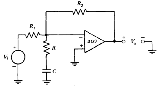
Figure 13.1 Lag compensation for the inverting amplifier connection.
Figure 13.1 illustrates the topology for lag compensating the inverting connection. The loop transmission for this system (assuming that loading at the input and the output of the amplifier is insignificant) is
\[L(s) = -\dfrac{a(s) R_1}{(R_1 + R_2)} \dfrac{(RCs + 1)}{[(R_1 ||R_2 + R) Cs + 1]} \nonumber \]
The dynamics of this loop transmission include a lag transfer function with a pole located at \(s = -[1/(R_1 || R_2 R) C]\) and a zero located at \(s = -1/RC\).
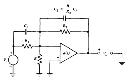
Figure 13.2 Lead compensation for the inverting amplifier connection.
The example of lead compensation using the topology shown in Figure 5.11 obtained the lead transfer function by paralleling one of the feedback-network resistors with a capacitor. A potential difficulty with this approach is that the ideal closed-loop transfer function is changed. An alternative is illustrated in Figure 13.2. Since component values are selected so that \(R_1 C_1 = R_2 C_2\), the ideal closed-loop transfer function is
\[\dfrac{V_o (s)}{V_i (s)} = -\dfrac{}{} = -\dfrac{R_2}{R_1} \nonumber \]
The loop transmission for this connection in the absence of loading and following some algebraic manipulation is
\[L(s) = -\dfrac{a(s) R_1 R}{(R_1 R_2 + R_1 R + R_2 R)} \dfrac{[(R_1 C_1)s + 1]}{[(R_1 || R_2 || R)(C_1 + C_2)s + 1]} \nonumber \]
A disadvantage of this method is that it lowers d-c loop-transmission magnitude compared with the topology that shunts \(R_2\) only with a capacitor. The additional attenuation that this method introduces beyond that provided by the \(R_1 -R_2\) network is equal to the ratio of the two break frequencies of the lead transfer function.
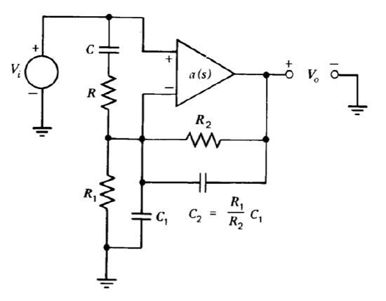
Figure 13.3 Lead and lag compensation for the noninverting amplifier connection.
This basic approach can also be used to combine lead and lag transfer functions in one loop transmission. Figure 13.3 illustrates one possibility for a noninverting connection. The equality of time constants in the feedback network insures that the ideal gain for this connection is
\[\dfrac{V_o (s)}{V_i (s)} = \dfrac{R_1 + R_2}{R_1} \nonumber \]
Some algebraic reduction indicates that the loop transmission (assuming negligible loading) is
\[L(s) = -\dfrac{a(s)R_1}{(R_1 + R_2)} \dfrac{(RCs + 1)(R_1 C_1 s + 1)}{\{R R_1 C C_1 s^2 + [(R_1 || R_2 + R)C + R_1 C_1]s + 1\}} \nonumber \]
The constraints among coefficients in the transfer function related to the feedback and shunt networks guarantee that this expression can be factored into a lead and a lag transfer function, and that the ratios of the singularity locations will be identical for the lead and the lag functions.
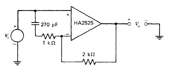
Figure 13.4 Unity-gain follower with input compensation.
The way that topologies of the type described above are used depends on the dynamics of the amplifier to be compensated and the load connected to it. For example, the HA2525 is a monolithic operational amplifier (made by a process more involved than the six-mask epitaxial process) that combines a unity-gain frequency of 20 MHz with a slew rate of 120 volts per microsecond. The dynamics of this amplifier are such that stability is guaranteed only for loop transmissions that combine the amplifier open-loop transfer function with an attenuation of three or more. Figure 13.4 shows how a stable, unity-gain follower can be constructed using this amplifier. Component values are selected so that the zero of the lag network is located approximately one decade below the compensated loop-transmission crossover frequency. Of course, the capacitor could be replaced by the short circuit, thereby lowering loop-transmission magnitude at all frequencies. However, advantages of the lag network shown include greater desensitivity at intermediate and low frequencies and lower output offset for a given offset referred to the input of the amplifier.
There are many variations on the basic theme of compensating with a network shunted across the input terminals of an operational amplifier. For example, many amplifiers with fixed transfer functions are designed to be stable with direct feedback provided that the unloaded open-loop transfer function of the amplifier is not altered by loading. However, a load capacitor can combine with the openloop output resistance of the amplifier to create a pole that compromises stability. Performance can often be improved in these cases by using lead input compensation to offset the effects of the second pole in the vicinity of the crossover frequency or by using lag input compensation to force crossover below the frequency where the pole associated with the load becomes important.
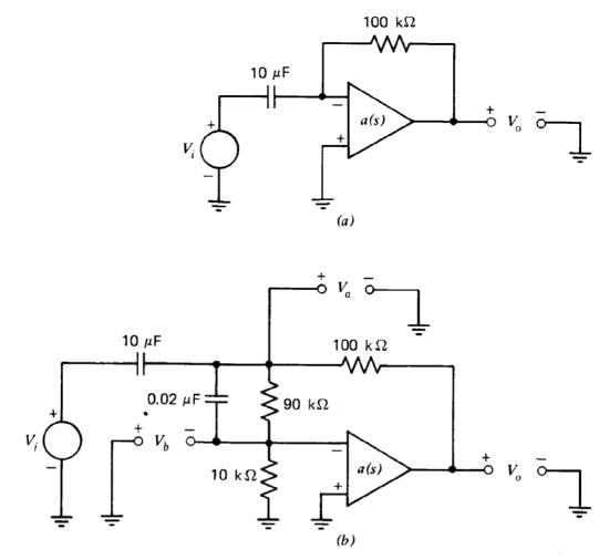
Figure 13.5 Differentiator. (\(a\)) Uncompensated. (\(b\)) With input lead compensation.
In other connections, an additional pole that deteriorates stability results from the feedback network. As an example, consider the differentiator shown in Figure 13.5\(a\). The ideal closed-loop transfer function for this connection is
\[\dfrac{V_o (s)}{V_i (s)} = -s \nonumber \]
It should be noted at the outset that this connection is not recommended since, in addition-to its problems with stability, the differentiator is an inherently noisy circuit. The reason is that differentiation accentuates the input noise of the amplifier because the ideal gain of a differentiator is a linearly increasing function of frequency.
Many amplifiers are compensated to have an approximately single-pole open-loop transfer function, since this type of transfer function results in excellent stability provided that the load element and the feedback network do not introduce additional poles. Accordingly, we assume that for the amplifier shown in Figure 13.5\(a\)
\[a(s) = \dfrac{10^5}{0.01s + 1} \nonumber \]
If loading is negligible, the feedback network and the amplifier open-loop transfer function combine to produce the loop transmission
\[L(s) = -\dfrac{10^5}{(0.01 s + 1)(s + 1)} \nonumber \]
The unity-gain frequency of this function is \(3.16 \times 10^3\) radians per second and its phase margin is less than \(2^{\circ}\).
Stability is improved considerably if the network shown in Figure 13.5\(b\) is added at the input of the amplifier. In the vicinity of the crossover frequency, the impedance of the \(10-\mu F\) capacitor (which is approximately equal to the Thevenin-equivalent impedance facing the compensating network) is much lower than that of the network itself. Accordingly the transfer function from \(V_o (s)\) to \(V_a (s)\) is not influenced by the input network at these frequencies. The lead transfer function that relates \(V_b (s)\) to \(V_a (S)\) combines with other elements in the loop to yield a loop transmission in the vicinity of the crossover frequency
\[L(s) \simeq -\dfrac{10^6 (1.8 \times 10^{-3} s + 1)}{s^2 (1.8 \times 10^{-4} s + 1)}\label{eq13.2.9} \]
(Note that this expression has been simplified by recognizing that at frequencies well above 100 radians per second, the two low-frequency poles can be considered located at the origin with appropriate modification of the scale factor.) The unity-gain frequency of Equation \(\ref{eq13.2.9}\) is \(1.8 \times 10^3\) radians per second, or approximately the geometric mean of the singularities of the lead network. Thus (from Equation 5.2.6) the phase margin of this system is \(55^{\circ}\).
One problem with the circuit shown in Figure 13.5\(b\) is that its output voltage offset is 20 times larger than the offset referred to the input of the amplifier. The output offset can be made equal to amplifier input offset by including a capacitor in series with the \(10-k\Omega\) resistor, thereby introducing both lead and lag transfer functions with the input network. If the added capacitor has negligibly low impedance at the crossover frequency, phase margin is not changed by this modification. In order to prevent conditional stability this capacitor should be made large enough so that the phase shift of the negative of the loop transmission does not exceed \(-180^{\circ}\) at low frequencies.
Other Methods
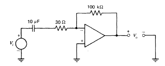
The preceding section focused on the use of a shunt network at the input of the operational amplifier to modify the loop transmission. In certain other cases, the feedback network can be changed to improve stability without significantly altering the ideal closed-loop transfer function. As an example, consider the circuit shown in Figure 13.6. The ideal closed-loop transfer function for this circuit is
\[\dfrac{V_o (s)}{V_i (s)} = -\dfrac{s}{3 \times 10^{-4} s + 1} \nonumber \]
and thus it functions as a differentiator at frequencies well below \(3.3 \times 10^3\) radians per second. The transfer function from the output of the operational amplifier to its inverting input via the feedback network includes a zero because of the \(30-\Omega\) resistor. The resulting loop transmission is
\[L(s) = -\dfrac{a(s) (3 \times 10^{-4} s + 1)}{s + 1} \label{eq13.2.11} \]
If it is assumed that the amplifier open-loop transfer function is the same as in the previous differentiator example \([a(s) = 10^5/(0.01s + 1)]\), Equation \(\ref{eq13.2.11}\) becomes
\[L(s) \simeq -\dfrac{10^7 (3 \times 10^{-4} s + 1)}{s^2}\label{eq13.2.12} \]
in the vicinity of the unity-gain frequency. The unity-gain frequency for Equation \(\ref{eq13.2.12}\) is approximately \(4 \times 10^3\) radians per second and the phase margin is \(50^{\circ}\). Thus the differentiator connection of Figure 13.6 combines stability comparable to that of the earlier example with a higher crossover frequency. While the ideal closed-loop gain includes a pole, the pole location is above the crossover frequency of the previous connection. Since the actual closed-loop gain of any feedback system departs substantially from its ideal value at the crossover frequency, this approach can yield performance superior to that of the circuit shown in Figure 13.5.
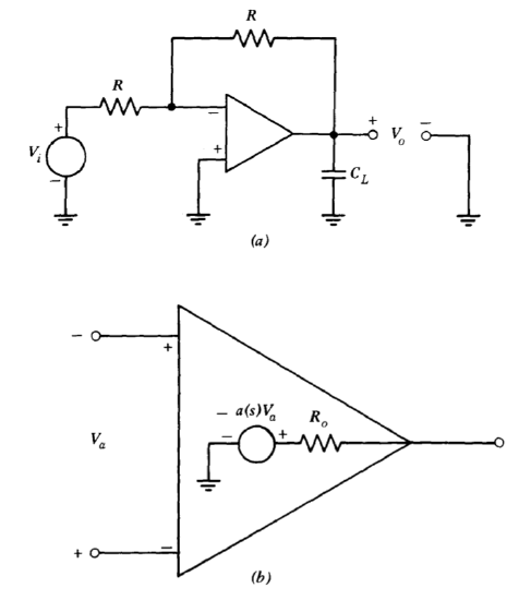
Figure 13.7 Capacitively loaded inverter. (\(a\)) Circuit. (\(b\)) Amplifier model.
In the examples involving differentiation, loop stability was compromised by a pole introduced by the feedback network. Another possibility is that a capacitive load adds a pole to the loop-transmission expression. Consider the capacitively loaded inverter shown in Figure 13.7. The additional pole results because the amplifier has nonzero output resistance (see the amplifier model of Figure 13.7\(b\)). If the resistor value \(R\) is much larger than \(R_o\) and loading at the input of the amplifier is negligible, the loop transmission is
\[L(s) = -\dfrac{a(s)}{2(R_o C_L s + 1)} \nonumber \]
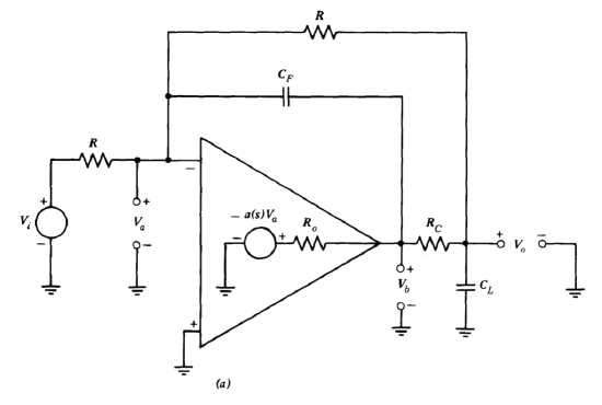
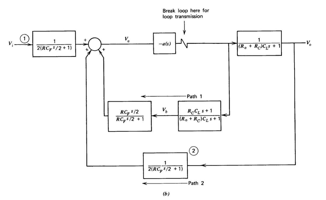
Figure 13.8 Feedback-network compensation for capacitively loaded inverter. (\(a\)) Circuit. (\(b\)) Block diagram.
The feedback-path connection can be modified as shown in Figure 13.8\(a\) to improve stability. It is assumed that parameter values are selected so that \(R \gg R_o + R_C\) and that the impedance of capacitor \(C_F\) is much larger in magnitude than \(R_o\) at all frequencies of interest. With these assumptions, the equations for the circuit are
\[V_a = \dfrac{(V_i + V_o)}{2[(RC_F/2)s + 1]} + \dfrac{V_b (RC_F/2)s}{(RC_F/2)s + 1} \nonumber \]
\[V_b = \dfrac{a(s) V_a (R_C C_L s + 1)}{(R_o + R_C) C_L s + 1} \nonumber \]
\[V_o = -\dfrac{a(s) V_a}{(R_o + R_C) C_L s + 1} \nonumber \]
These equations lead to the block diagram shown in Figure 13.8\(b\).
Two important features are evident from the block diagram or from physical arguments based on the circuit configuration. First, since the transfer functions of blocks ① and ② are identical and since the outputs of both of these blocks are summed with the same sign to obtain \(V_a\), the ideal output is the negative of the input at frequencies where the signal propagated through path 1 is insignificant. We can argue the same result physically, since Figure 13.8\(a\) indicates an ideal transfer function \(V_o = - V_i\) if feedback through \(C_F\) is negligible.
The second conclusion involves the stability of the system. If the loop is broken at the indicated point, the loop transmission is
\[\begin{array} {rcl} {L(s)} & = & {-a(s) \underbrace{\dfrac{[(RC_F/2)s]}{[(RC_F/2)s + 1]} \dfrac{(R_C C_L s + 1)}{[(R_o + R_C) C_L s + 1]}}_{\text{term from feedback via path 1}}} \\ {} & \ & {-\underbrace{\dfrac{a(s)}{2[(R_o + R_C)C_L s + 1][(RC_F/2)s + 1]}}_{\text{term from feedback via path 2}}}\end{array} \label{eq13.2.15} \]
At sufficiently high frequencies, Equation \(\ref{eq13.2.15}\) reduces to
\[L(s) \simeq -\dfrac{a(s) R_C}{R_o + R_C}\label{eq13.2.16} \]
because path transmission of path 1 reaches a constant value, while that of path 2 is progressively attenuated with frequency. If parameters are chosen so that crossover occurs where the approximation of Equation \(\ref{eq13.2.16}\) is valid, system stability is essentially unaffected by the load capacitor. The same result can be obtained directly from the circuit of Figure 13.8\(a\). If parameters are chosen so that at the crossover frequency \(\omega_c\)
\[\dfrac{1}{C_L \omega_c} \ll R_o + R_C \ \ \text{ and } \ \ R_o \ll \dfrac{1}{C_F \omega_c} \ll \dfrac{R}{2}\nonumber \]
the feedback path around the amplifier is frequency independent at crossover.
Previous examples have indicated how dynamics related to the feedback network or the load can deteriorate stability. Stability may also suffer if an active element that provides voltage gain greater than one is used in the feedback path, since this type of feedback element will result in a loop- transmission crossover frequency in excess of the unity-gain frequency of the operational amplifier itself. Additional negative phase shift then occurs at crossover because the higher-frequency poles of the amplifier open-loop transfer function are significant at the higher crossover frequency.
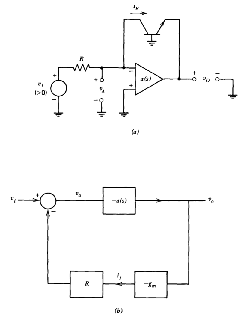
Figure 13.9 Evaluation of log-circuit stability. (\(a\)) Circuit. (\(b\)) Linearized block diagram.
The simple log circuit described in Section 11.5.4 demonstrates this type of difficulty. The basic circuit is illustrated in Figure 13.9\(a\). We recall that the ideal input-output transfer relationship for this circuit is
\[v_O = -\dfrac{kT}{q} \ln \dfrac{v_I}{RI_S} \nonumber \]
where the quantity \(I_s\) characterizes the transistor.
A linearized block diagram for the connection, formed assuming that loading at the input and the output of the amplifier is negligible, is shown in Figure 13.9\(b\). Since the quiescent collector current of the transistor is related to the operating-point value of the input voltage \(V_I\) by \(I_F = V_I/R\), the transistor transconductance is
\[g_m = \dfrac{qV_I}{kTR} \nonumber \]
Consequently, the loop transmission for the linearized system is
\[L(s) = -a(s) \dfrac{qV_I}{kT} \nonumber \]
If it is assumed that the maximum operating-point value of the input signal is 10 volts, the feedback network can provide a voltage gain of as much as 400. It is clear that few amplifiers with fixed open-loop transfer functions will be compensated conservatively enough to remain stable with this increase in loop-transmission magnitude.
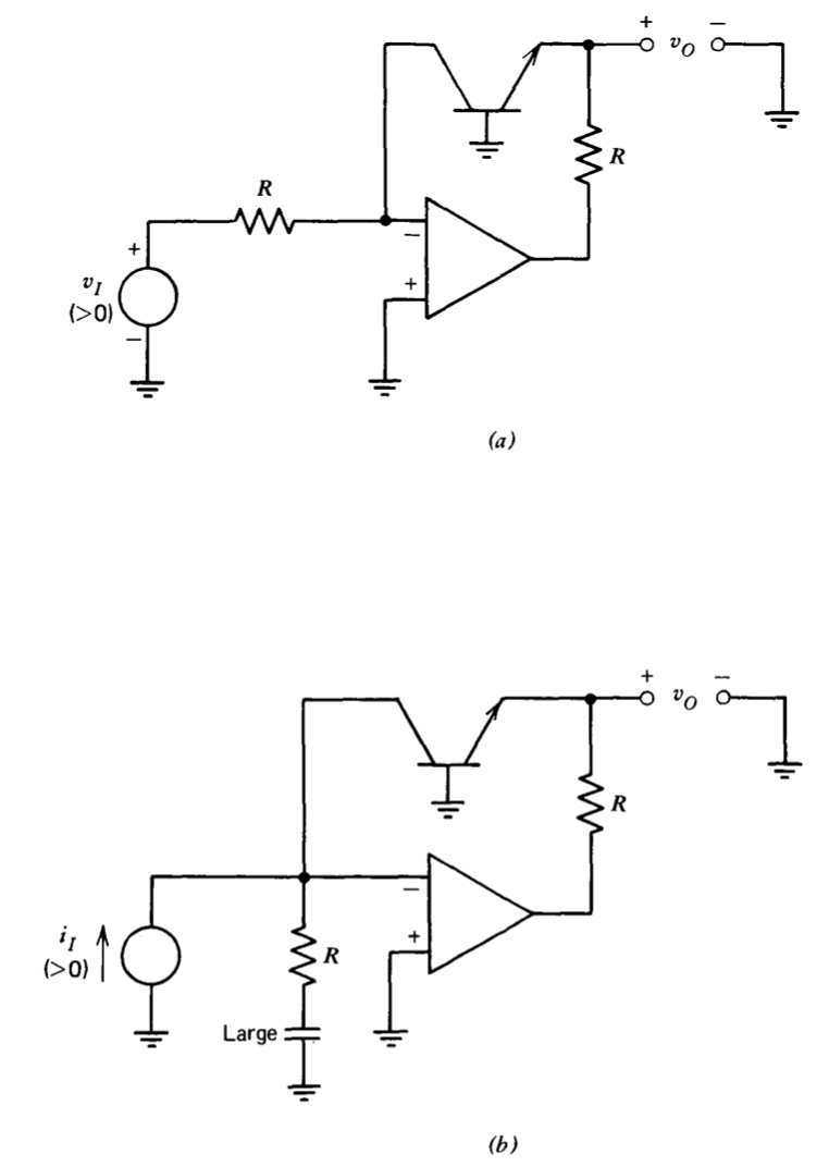
Figure 13.10 Reduction of loop-transmission magnitude for log circuit. (\(a\)) Use of emitter resistor. (\(b\)) Emitter resistor combined with input lag compensation.
A method that can be used to reduce the high voltage gain of the feedback network is illustrated in Figure 13.10. By including a transistor emitter resistor equal in value to the input resistor, we find that the maximum voltage gain of the resultant common-base amplifier is reduced to one. Note that the feedback effectively constrains the voltage at the emitter of the transistor to be logarithmically related to input voltage independent of load current, and thus the ideal transfer relationship of the circuit is independent of load. Also note that at least in the absence of significant output- current drain, the maximum voltage across the emitter resistor is equal to the maximum input voltage so that output-voltage range is often unchanged by this modification.
It was mentioned in Section 11.5.4 that the log circuit can exhibit very wide dynamic range when the input signal is supplied from a current source, since the voltage offset of the amplifier does not give rise to an error current in this case. Figure 13.10\(b\) shows how input lag compensation can be combined with emitter degeneration to constrain loop-transmission magnitude without deteriorating dynamic range for current-source inputs.