
24.8: Questions
- Page ID
- 32723
")
\( \newcommand{\vecs}[1]{\overset { \scriptstyle \rightharpoonup} {\mathbf{#1}} } \)
\( \newcommand{\vecd}[1]{\overset{-\!-\!\rightharpoonup}{\vphantom{a}\smash {#1}}} \)
\( \newcommand{\dsum}{\displaystyle\sum\limits} \)
\( \newcommand{\dint}{\displaystyle\int\limits} \)
\( \newcommand{\dlim}{\displaystyle\lim\limits} \)
\( \newcommand{\id}{\mathrm{id}}\) \( \newcommand{\Span}{\mathrm{span}}\)
( \newcommand{\kernel}{\mathrm{null}\,}\) \( \newcommand{\range}{\mathrm{range}\,}\)
\( \newcommand{\RealPart}{\mathrm{Re}}\) \( \newcommand{\ImaginaryPart}{\mathrm{Im}}\)
\( \newcommand{\Argument}{\mathrm{Arg}}\) \( \newcommand{\norm}[1]{\| #1 \|}\)
\( \newcommand{\inner}[2]{\langle #1, #2 \rangle}\)
\( \newcommand{\Span}{\mathrm{span}}\)
\( \newcommand{\id}{\mathrm{id}}\)
\( \newcommand{\Span}{\mathrm{span}}\)
\( \newcommand{\kernel}{\mathrm{null}\,}\)
\( \newcommand{\range}{\mathrm{range}\,}\)
\( \newcommand{\RealPart}{\mathrm{Re}}\)
\( \newcommand{\ImaginaryPart}{\mathrm{Im}}\)
\( \newcommand{\Argument}{\mathrm{Arg}}\)
\( \newcommand{\norm}[1]{\| #1 \|}\)
\( \newcommand{\inner}[2]{\langle #1, #2 \rangle}\)
\( \newcommand{\Span}{\mathrm{span}}\) \( \newcommand{\AA}{\unicode[.8,0]{x212B}}\)
\( \newcommand{\vectorA}[1]{\vec{#1}} % arrow\)
\( \newcommand{\vectorAt}[1]{\vec{\text{#1}}} % arrow\)
\( \newcommand{\vectorB}[1]{\overset { \scriptstyle \rightharpoonup} {\mathbf{#1}} } \)
\( \newcommand{\vectorC}[1]{\textbf{#1}} \)
\( \newcommand{\vectorD}[1]{\overrightarrow{#1}} \)
\( \newcommand{\vectorDt}[1]{\overrightarrow{\text{#1}}} \)
\( \newcommand{\vectE}[1]{\overset{-\!-\!\rightharpoonup}{\vphantom{a}\smash{\mathbf {#1}}}} \)
\( \newcommand{\vecs}[1]{\overset { \scriptstyle \rightharpoonup} {\mathbf{#1}} } \)
\(\newcommand{\longvect}{\overrightarrow}\)
\( \newcommand{\vecd}[1]{\overset{-\!-\!\rightharpoonup}{\vphantom{a}\smash {#1}}} \)
\(\newcommand{\avec}{\mathbf a}\) \(\newcommand{\bvec}{\mathbf b}\) \(\newcommand{\cvec}{\mathbf c}\) \(\newcommand{\dvec}{\mathbf d}\) \(\newcommand{\dtil}{\widetilde{\mathbf d}}\) \(\newcommand{\evec}{\mathbf e}\) \(\newcommand{\fvec}{\mathbf f}\) \(\newcommand{\nvec}{\mathbf n}\) \(\newcommand{\pvec}{\mathbf p}\) \(\newcommand{\qvec}{\mathbf q}\) \(\newcommand{\svec}{\mathbf s}\) \(\newcommand{\tvec}{\mathbf t}\) \(\newcommand{\uvec}{\mathbf u}\) \(\newcommand{\vvec}{\mathbf v}\) \(\newcommand{\wvec}{\mathbf w}\) \(\newcommand{\xvec}{\mathbf x}\) \(\newcommand{\yvec}{\mathbf y}\) \(\newcommand{\zvec}{\mathbf z}\) \(\newcommand{\rvec}{\mathbf r}\) \(\newcommand{\mvec}{\mathbf m}\) \(\newcommand{\zerovec}{\mathbf 0}\) \(\newcommand{\onevec}{\mathbf 1}\) \(\newcommand{\real}{\mathbb R}\) \(\newcommand{\twovec}[2]{\left[\begin{array}{r}#1 \\ #2 \end{array}\right]}\) \(\newcommand{\ctwovec}[2]{\left[\begin{array}{c}#1 \\ #2 \end{array}\right]}\) \(\newcommand{\threevec}[3]{\left[\begin{array}{r}#1 \\ #2 \\ #3 \end{array}\right]}\) \(\newcommand{\cthreevec}[3]{\left[\begin{array}{c}#1 \\ #2 \\ #3 \end{array}\right]}\) \(\newcommand{\fourvec}[4]{\left[\begin{array}{r}#1 \\ #2 \\ #3 \\ #4 \end{array}\right]}\) \(\newcommand{\cfourvec}[4]{\left[\begin{array}{c}#1 \\ #2 \\ #3 \\ #4 \end{array}\right]}\) \(\newcommand{\fivevec}[5]{\left[\begin{array}{r}#1 \\ #2 \\ #3 \\ #4 \\ #5 \\ \end{array}\right]}\) \(\newcommand{\cfivevec}[5]{\left[\begin{array}{c}#1 \\ #2 \\ #3 \\ #4 \\ #5 \\ \end{array}\right]}\) \(\newcommand{\mattwo}[4]{\left[\begin{array}{rr}#1 \amp #2 \\ #3 \amp #4 \\ \end{array}\right]}\) \(\newcommand{\laspan}[1]{\text{Span}\{#1\}}\) \(\newcommand{\bcal}{\cal B}\) \(\newcommand{\ccal}{\cal C}\) \(\newcommand{\scal}{\cal S}\) \(\newcommand{\wcal}{\cal W}\) \(\newcommand{\ecal}{\cal E}\) \(\newcommand{\coords}[2]{\left\{#1\right\}_{#2}}\) \(\newcommand{\gray}[1]{\color{gray}{#1}}\) \(\newcommand{\lgray}[1]{\color{lightgray}{#1}}\) \(\newcommand{\rank}{\operatorname{rank}}\) \(\newcommand{\row}{\text{Row}}\) \(\newcommand{\col}{\text{Col}}\) \(\renewcommand{\row}{\text{Row}}\) \(\newcommand{\nul}{\text{Nul}}\) \(\newcommand{\var}{\text{Var}}\) \(\newcommand{\corr}{\text{corr}}\) \(\newcommand{\len}[1]{\left|#1\right|}\) \(\newcommand{\bbar}{\overline{\bvec}}\) \(\newcommand{\bhat}{\widehat{\bvec}}\) \(\newcommand{\bperp}{\bvec^\perp}\) \(\newcommand{\xhat}{\widehat{\xvec}}\) \(\newcommand{\vhat}{\widehat{\vvec}}\) \(\newcommand{\uhat}{\widehat{\uvec}}\) \(\newcommand{\what}{\widehat{\wvec}}\) \(\newcommand{\Sighat}{\widehat{\Sigma}}\) \(\newcommand{\lt}{<}\) \(\newcommand{\gt}{>}\) \(\newcommand{\amp}{&}\) \(\definecolor{fillinmathshade}{gray}{0.9}\)Quick questions
You should be able to answer these questions without too much difficulty after studying this TLP. If not, then you should go through it again!
Which force/forces act on metal ions within a conductor, during electromigration – under the application of an electric field? (You may pick more than one answer)
(a) Wind force, F = aneλdσijρ
(b) Direct force, F = aZejρ
(c) Mechanical back force, F = ΩΔσ/Δx
(d) Moment force, F = Moment/distance from pivot
(e) None of the above
- Answer
-
(a) wind force – scattering electron events within the conductor result in exerting a force on the metal ion.
(b) direct force – due to the electrostatic pull from the electric field.
(c) mechanical back force – results from the build up of stresses as mass atomic migration takes place within the conductor.
The median life of pure Al stripes of width, w (in cm) and thickness, d (in cm) at 50 °C is given by:
t50 = 4.4×10¹²wdj–n exp(Ee/kT)
where n = 2, Ee = 0.49 eV, j = 1 x 10⁵ A cm-2, w = 0.4 μm and d = 0.5 μm.
What is the median life of the interconnect?
(a) 0.38 hrs
(b) 3.83 hrs
(c) 38.3 hrs
(d) 380 hrs
Hint: Ensure that you are using the correct units:
w is in cm (4 × 10⁻⁵ cm) and d is in cm (5 × 10⁻⁵ cm).
T is in K (323 K)
Ee needs to be converted from eV to J using the relation: 1 eV = 1.6 x 10⁻¹⁹ J.
k = 1.38 x 10⁻²³ J K-1
- Answer
-
(c) 38.3 hrs
How does the median life of pure Al stripes compare with that of Al-Si interconnects of the same dimensions as above, for which:
\[t_{50}=2.2 \times 10^{15} \mathrm{wdj}^{-\mathrm{n}} \exp (0.54 \mathrm{eV} / \mathrm{kT})\]
- Answer
-
D
Which material properties are desirable for use as interconnects?
- Answer
-
B
Which material is the mostly used in vias?
- Answer
-
A
Deeper questions
The following questions require some thought and reaching the answer may require you to think beyond the contents of this TLP.
In a solid conductor, the mechano diffusion force, Fm, acting on an atom, in a gradient of hydrostatic stress, dσH / dx, is given by:
\[F_{m}=\frac{1}{C_{0}} \frac{d \sigma_{H}}{d x}\]
where C0 = no. of atoms per unit volume.
A conductor has along it, a segment of length, L, which has a raised atomic diffusivity. The material of the conductor develops damage when the difference in hydrostatic stress between the ends of such a segment reaches the value (ΔσH)crit. Derive the critical condition for the damage to develop in terms of L and current density, j, in the conductor.
- Answer
-
The mechano diffusion force, Fm, opposes the electromigration force Fwind +Fdirect = Z*ejρ.
At L and (ΔσH)crit damage is not yet observed. Above this critical value, damage would occur. Therefore at this point, both forces have to be equal and opposite:\[\frac{1}{C_{0}} \frac{d \sigma_{H}}{d x}=Z^{*} e \rho j\]
Assuming (dσH / dx) can be approximated to (ΔσH)crit / L,
\[\frac{1}{C_{0}} \frac{\Delta \sigma_{h, r r i t}}{L}=Z^{*} e \rho j\]
\[(j L)=\frac{1}{C_{0}} \frac{\Delta \sigma_{H, c r i t}}{Z^{*} e \rho}\]
This is the critical condition for damage to develop.
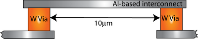
An IC has several levels of Al-based metallization linked by W vias. In a test, electromigration damage, develops in an Al-based conductor linking two vias when the current density flowing through it from one via to the other 10 μm away exceeds 9×10⁹ A m-2. It is planned to use the same materials with a current density of 1.2×10¹⁰ A m-2. What condition must be met by the length of links between vias for damage to be avoided? How will the temperature of the operation affect the development of electromigration damage?
- Answer
-
The critical condition for damage to develop within the system is:
(jL)crit = (9×10⁹)(10×10-6) = 90,000
Therefore to avoid any damage, the jL product has to be below the critical value. For current density, j = 1.2×10¹⁰:
jL = 90,000
1.2×10¹⁰L = 90,000
L = 7.5×10⁻⁶ mTherefore, in order for damage to be avoided, the length must be below 7.5 μm. This ensures that the mechano diffusion forces counters the electromigration force, thus preventing damage.
The flux of atoms is dependent on temperature, within the terms of D = D0exp(E/kT) and T. Therefore a higher temperature results in a faster rate of flux and faster occurrence of electromigration damage.
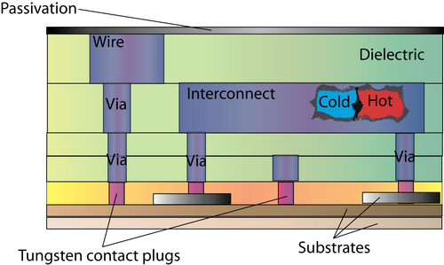
In the schematic diagram of a microelectronic device (below), where would electromigration-induced damage be observed? Give your reasons. What type of material would you use for the vias and interconnects, and why?
- Answer
-
The answers are marked in the diagram below:
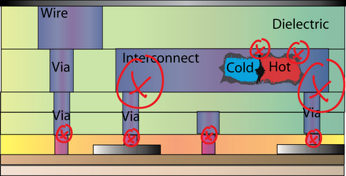
1. Interface between the tungsten and metallic via – differences in diffusivity rates result in negligible electromigration within tungsten, whilst atomic migration occurs in the metallic via.
2. Hot and cold regions within the metallization line – different rates of atomic migration result in an overall atomic flux, where hillocks and voids form in volumes of mass accumulation and depletion.
3. Bends within the metallization line – a decrease in metallization cross-sectional area results in an increase in Joule-heating and temperature. Current crowding takes place causing a flux divergence.
Cu is the most suitable for use as interconnects and vias, as it has a low resistivity (ρ = 1.67 μΩ cm), is resistant to electromigration, is easily processed into metallization lines (using newly developed technology) and is a relatively cheap material.
Alternatively, Al-Cu can be used for interconnects, coupled with W vias. This combination is less electromigration resistive than Cu.