
Nonideal PN Junction Diodes
- Page ID
- 368
\( \newcommand{\vecs}[1]{\overset { \scriptstyle \rightharpoonup} {\mathbf{#1}} } \)
\( \newcommand{\vecd}[1]{\overset{-\!-\!\rightharpoonup}{\vphantom{a}\smash {#1}}} \)
\( \newcommand{\dsum}{\displaystyle\sum\limits} \)
\( \newcommand{\dint}{\displaystyle\int\limits} \)
\( \newcommand{\dlim}{\displaystyle\lim\limits} \)
\( \newcommand{\id}{\mathrm{id}}\) \( \newcommand{\Span}{\mathrm{span}}\)
( \newcommand{\kernel}{\mathrm{null}\,}\) \( \newcommand{\range}{\mathrm{range}\,}\)
\( \newcommand{\RealPart}{\mathrm{Re}}\) \( \newcommand{\ImaginaryPart}{\mathrm{Im}}\)
\( \newcommand{\Argument}{\mathrm{Arg}}\) \( \newcommand{\norm}[1]{\| #1 \|}\)
\( \newcommand{\inner}[2]{\langle #1, #2 \rangle}\)
\( \newcommand{\Span}{\mathrm{span}}\)
\( \newcommand{\id}{\mathrm{id}}\)
\( \newcommand{\Span}{\mathrm{span}}\)
\( \newcommand{\kernel}{\mathrm{null}\,}\)
\( \newcommand{\range}{\mathrm{range}\,}\)
\( \newcommand{\RealPart}{\mathrm{Re}}\)
\( \newcommand{\ImaginaryPart}{\mathrm{Im}}\)
\( \newcommand{\Argument}{\mathrm{Arg}}\)
\( \newcommand{\norm}[1]{\| #1 \|}\)
\( \newcommand{\inner}[2]{\langle #1, #2 \rangle}\)
\( \newcommand{\Span}{\mathrm{span}}\) \( \newcommand{\AA}{\unicode[.8,0]{x212B}}\)
\( \newcommand{\vectorA}[1]{\vec{#1}} % arrow\)
\( \newcommand{\vectorAt}[1]{\vec{\text{#1}}} % arrow\)
\( \newcommand{\vectorB}[1]{\overset { \scriptstyle \rightharpoonup} {\mathbf{#1}} } \)
\( \newcommand{\vectorC}[1]{\textbf{#1}} \)
\( \newcommand{\vectorD}[1]{\overrightarrow{#1}} \)
\( \newcommand{\vectorDt}[1]{\overrightarrow{\text{#1}}} \)
\( \newcommand{\vectE}[1]{\overset{-\!-\!\rightharpoonup}{\vphantom{a}\smash{\mathbf {#1}}}} \)
\( \newcommand{\vecs}[1]{\overset { \scriptstyle \rightharpoonup} {\mathbf{#1}} } \)
\(\newcommand{\longvect}{\overrightarrow}\)
\( \newcommand{\vecd}[1]{\overset{-\!-\!\rightharpoonup}{\vphantom{a}\smash {#1}}} \)
\(\newcommand{\avec}{\mathbf a}\) \(\newcommand{\bvec}{\mathbf b}\) \(\newcommand{\cvec}{\mathbf c}\) \(\newcommand{\dvec}{\mathbf d}\) \(\newcommand{\dtil}{\widetilde{\mathbf d}}\) \(\newcommand{\evec}{\mathbf e}\) \(\newcommand{\fvec}{\mathbf f}\) \(\newcommand{\nvec}{\mathbf n}\) \(\newcommand{\pvec}{\mathbf p}\) \(\newcommand{\qvec}{\mathbf q}\) \(\newcommand{\svec}{\mathbf s}\) \(\newcommand{\tvec}{\mathbf t}\) \(\newcommand{\uvec}{\mathbf u}\) \(\newcommand{\vvec}{\mathbf v}\) \(\newcommand{\wvec}{\mathbf w}\) \(\newcommand{\xvec}{\mathbf x}\) \(\newcommand{\yvec}{\mathbf y}\) \(\newcommand{\zvec}{\mathbf z}\) \(\newcommand{\rvec}{\mathbf r}\) \(\newcommand{\mvec}{\mathbf m}\) \(\newcommand{\zerovec}{\mathbf 0}\) \(\newcommand{\onevec}{\mathbf 1}\) \(\newcommand{\real}{\mathbb R}\) \(\newcommand{\twovec}[2]{\left[\begin{array}{r}#1 \\ #2 \end{array}\right]}\) \(\newcommand{\ctwovec}[2]{\left[\begin{array}{c}#1 \\ #2 \end{array}\right]}\) \(\newcommand{\threevec}[3]{\left[\begin{array}{r}#1 \\ #2 \\ #3 \end{array}\right]}\) \(\newcommand{\cthreevec}[3]{\left[\begin{array}{c}#1 \\ #2 \\ #3 \end{array}\right]}\) \(\newcommand{\fourvec}[4]{\left[\begin{array}{r}#1 \\ #2 \\ #3 \\ #4 \end{array}\right]}\) \(\newcommand{\cfourvec}[4]{\left[\begin{array}{c}#1 \\ #2 \\ #3 \\ #4 \end{array}\right]}\) \(\newcommand{\fivevec}[5]{\left[\begin{array}{r}#1 \\ #2 \\ #3 \\ #4 \\ #5 \\ \end{array}\right]}\) \(\newcommand{\cfivevec}[5]{\left[\begin{array}{c}#1 \\ #2 \\ #3 \\ #4 \\ #5 \\ \end{array}\right]}\) \(\newcommand{\mattwo}[4]{\left[\begin{array}{rr}#1 \amp #2 \\ #3 \amp #4 \\ \end{array}\right]}\) \(\newcommand{\laspan}[1]{\text{Span}\{#1\}}\) \(\newcommand{\bcal}{\cal B}\) \(\newcommand{\ccal}{\cal C}\) \(\newcommand{\scal}{\cal S}\) \(\newcommand{\wcal}{\cal W}\) \(\newcommand{\ecal}{\cal E}\) \(\newcommand{\coords}[2]{\left\{#1\right\}_{#2}}\) \(\newcommand{\gray}[1]{\color{gray}{#1}}\) \(\newcommand{\lgray}[1]{\color{lightgray}{#1}}\) \(\newcommand{\rank}{\operatorname{rank}}\) \(\newcommand{\row}{\text{Row}}\) \(\newcommand{\col}{\text{Col}}\) \(\renewcommand{\row}{\text{Row}}\) \(\newcommand{\nul}{\text{Nul}}\) \(\newcommand{\var}{\text{Var}}\) \(\newcommand{\corr}{\text{corr}}\) \(\newcommand{\len}[1]{\left|#1\right|}\) \(\newcommand{\bbar}{\overline{\bvec}}\) \(\newcommand{\bhat}{\widehat{\bvec}}\) \(\newcommand{\bperp}{\bvec^\perp}\) \(\newcommand{\xhat}{\widehat{\xvec}}\) \(\newcommand{\vhat}{\widehat{\vvec}}\) \(\newcommand{\uhat}{\widehat{\uvec}}\) \(\newcommand{\what}{\widehat{\wvec}}\) \(\newcommand{\Sighat}{\widehat{\Sigma}}\) \(\newcommand{\lt}{<}\) \(\newcommand{\gt}{>}\) \(\newcommand{\amp}{&}\) \(\definecolor{fillinmathshade}{gray}{0.9}\)A p-n junction diode is a kind of semiconductor diode that made up of a joining p-type and n-type semiconducting layers. The current in the pn junction diode can only flow from one side to the other. An Ideal pn junction diode is based on the following basic assumption:
- The diode is in steady state conditions.
- The doping of the diode is a nondegenerately doped step junction.
- The diode is 1-D (one dimension).
- The quasineutral regions are in low-level injection.
- No other process than drift, diffusion, and thermal recombination-generation happen in the diode. GL=0.
However, some of the above assumption have not enough justifications. As a result, by analyzing the experimental I-V characteristics, the following possible sources for the deviations from the ideal pn junction diodes can happen:
- Avalanching
- Zener Process
- The R-G current
- Series Resistance
- High-Level Injection
Introduction
According to the ideal theory of pn junction, the forward current rises dramatically as a function of the applied voltage, while the reverse current vanishes in a very small amount. However, an obvious feature beyond the expectation of the ideal theory is observed in the experimental I-V curve: as the reverse voltage exceeds a specific value, a large reverse-bias current is generated. Such phenomenon is called breakdown. The value of breakdown voltage varies in large scientific orders, but the breakdown phenomenon occurs in all pn junction diodes, and addresses a major deviation from the ideal pn junction diodes.
For a certain range of forward bias voltage, the I-V curve follows the ideal theory. However, when the forward bias exceeds a certain value, the slop of the I-V curve decreases gradually from q/(kT). This phenomenon results from the high current in the device when VA goes to Vbi. For a very small forward bias, the observed I-V curve slope is approaching q/(2kT), which also results a deviations from the ideal theory. This phenomenon indicates a possible neglected current component in the ideal diode equation. Moreover, with reverse bias, the current does not saturate according to the ideal theory, but instead, increases along with the reverse bias. The carrier generation-recombination, which is neglected in the ideal pn junction theory, is responsible for the small continuously change in the reverse-bias and forward-bias differences from the ideal pn junction diode behaviors.
Reverse-Bias Breakdown
Given the term is called "breakdown", it is a reversible process that does not damage the diode. However, the current should be limited to prevent over heating. The breakdown voltage VBR in the reverse bias region indicates where the infinite current occurs. For a given doping level, VBR increases with the band gap of the semiconductor material in a diode. In addition, the doping in the light doping junction side (NB) can change the VBR over three orders of magnitude. The value of VBR is proportional to 1/NB0.75.
Two processes generate the breakdown current. One is called avalanching and the other is the Zener process. Generally, avalanching is the dominant source while the Zener process occurs only when the junction is doped heavily on both sides.
Avalanching
In ideal condition, when the applied voltage VA is much smaller than the breakdown voltage in the reverse bias, the reverse current results from the random motion of the minority carriers moving and accelerating in the depletion region from one side to the other due to the applied electric field. At small reverse biases, the energy lost of carries due to every collision between the carries and the semiconductor lattice is relatively small. Such energy just forms lattice vibrations as dispersible localized heating.
When the reverse bias continuously increases, the energy transferred in each collision becomes large enough to ionize a semiconductor atom-- the collision makes an electron jump from the valence band to the conduction band and therefore generates electron-hole pair. The impact ionization process described above creates carriers and immediately accelerated in with the applied bias in the depletion region. As a result, the generated carriers collide with the original carriers and form even more carriers, which can be visualized in Fig 1.
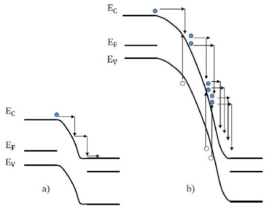
The exponential carrier creation consequently increases the reverse current to infinity. Without carrier multiplication, the multiplication factor M can be calculated with equation 1. The multiplication factor shows how current increase with the carrier multiplication.
\[ M={|I| \over I_0} \label{1}\]
However, the experimental data provides that
\[M=\frac{1}{1-\frac{|V_A|}{V_{BR}}^m} \label{2} \]
m is usually a value between 3 and 6, depending on the semiconductor types.
The breakdown voltage VBR is inversely proportional to the doping NB on the light dope side of the pn junction. Since VBR is dependent on the band gap, EG, of the semiconductor, the required ionization energy is also dependent on EG. Moreover, the VBR resulted from avalanching also increases with increasing temperature, because of the increasing lattice scattering caused by the increasing temperature. The increasing lattice scattering can cause a smaller mean free path and a larger avalanching critical electric field, both of which leads to a higher breakdown voltage.
Zener Process
The Zener process is a term used to indicate the "tunneling" process in a reverse-biased diode. The tunneling can be visualized with Figure 2.
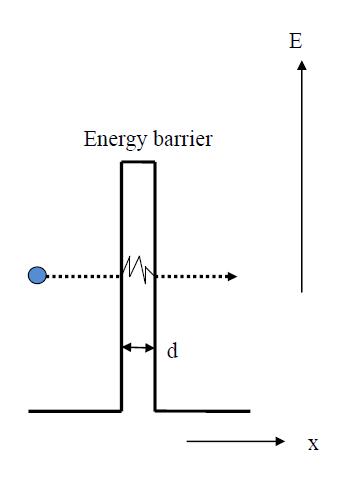
Tunneling occurs and becomes significant with the following two major requirement:
- For the barrier at the same energy, one side of the barrier contains filled states while the other one contains empty states. Tunneling will not occur in a region without allowed states.
- The potential barrier width d must be very thin, and the quantum mechanical tunneling only becomes important when d is smaller than 10-6 cm.
The Zener Process is visualized in figure 3. As the reverse bias becomes greater, the more filled valence electron states on the p-side than against the empty conduction band states on the n-side, so the magnitude of the reverse-bias tunneling current is larger.
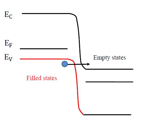
The tunneling is significant only when d is smaller than 10-6 cm which requires more than 1017/cm3 doping on the "lightly" doping side of the pn junction. So the Zenner Process only becomes significant when the diode is heavily doped on both sides of the junction. The Zener process contributes significantly when VBR<6EG/q and dominates when VBR <4EG/q. Compared with the avalanching, VBR decreases with increasing T if the Zener process dominates.
The Recombination-Generation (R-G) Current
For the small forward biases and all the reverse biases at room temperature, a current beyond the predicted values from the ideal diode theory was observed. Such current is formed by the thermal carrier recombination-generation in the depletion region, but such R-G process is neglected in the ideal diode theory. When the diode is applied reverse biasing, the carrier concentrations in the depletion region decreases below the equilibrium values, which causes the thermal generation of electrons and holes over the region. On the other hand, the forward biasing increases the carrier concentrations in the depletion region and leads to the carrier recombination in the same region.
High-Current Phenomena at Va-->Vbi
A significant deviation of current behavior occurs when the applied forward bias is close to Vbi. A large current drives the diode to behave in a way that beyond the ideal pn junction diode theory. Not all of the applied voltage is dropped across the depletion region when series resistance is taken into consideration. In addition, a large current can also generate a high injection level which is against one of the ideal diode assumptions.
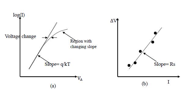
Series Resistance
The doping and the dimensions of the quasineutral regions provide the regions with an inherent resistance. In addition, a residual resistance related with the diode contacts is also contained in the device. Both of the resistance combine to be RS, which is the series resistance the current experience when it flow though the junction. At low current the voltage drop due to the series resistance is negligible; however, if the current is large enough so that IRS is comparable to VA the applied voltage drop should be modified to
VJ=VA-IRS
The following Figure 5 shows how the series resistance influences the I-V curve of the pn junction diodes.
High-Level Injection
When the minority carrier concentration at the edge of the depletion region on the side of lightly doping, the low-level injection assumption in the ideal diode theory fails. For example, for the Si at room temperature, when the applied voltage is a few tenths volt below Vbi. The deviation of high-level injection should be taken into consideration. Under high-level injection, the majority carrier concentration has to be increase to maintain the neutrality of charge in the quasineutral regions. A slope of q/2kT is predicted for the log(I) vs. V curve. However, such slope is seldom observed because of the effect of the series resistance. The high-level carrier injection can cause the decrease in resistivity due to the conductivity modulation.
Conclusion
Form the above analysis, the deviations of pn junction diodes can be conclude with the following table:
| Deviations from Ideal | Reasons | Results |
|---|---|---|
| Avalanching | impact ionization | infinite reverse-bias current (breakdown) |
| Zener Process | tunneling (high doped, thin barrier width) | infinite reverse-bias current (breakdown) |
| R-G Current | thermal R-G | slope changing in the semilog I-V curve in small forward/reverse biasing regions |
| Series Resistance | large current makes the resistance in the diode contacts significant | decrease in the slope of semilog I-V plot as VA goes to Vbi. |
| High-level Injection | majority carriers increase to neutralize the charge in quasineutral regions | slope of q/2kT region in the log(I) vs. V plot. |
Questions
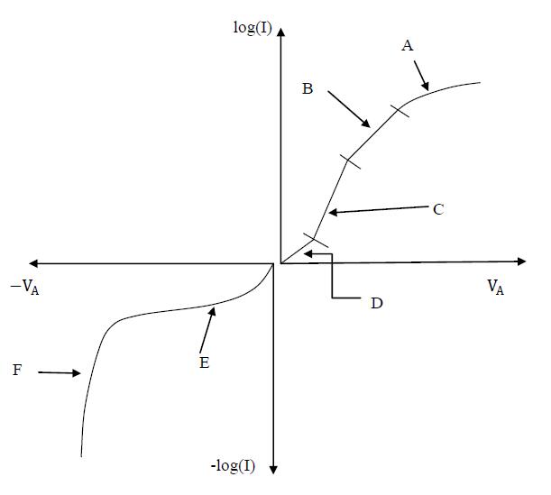
1. For the following Figure 7, label the missing part (A, B, C, D, E and F) with proper I-V features.
2. Why the predicted q/2kT region is seldom observed for high-level injection in the pn junction diodes?
3. Name the mechanisms that can make the current go to infinity under reverse bias.
Answers
1. A. Series resistance; B, High-level injection; C, Ideal region; D, Thermal recombination in the depletion region; E, Thermal generation in the depletion region; F, Avalanching and/or Zener process.
2. Because the effect is usually obscured by the effect of series resistance.
3. Avalanching and the Zener Process.
References
1. Robert F. Pierret, Semiconductor Device Fundamentals, Second Edition. Chapter 6, pages 235-300.
2. Ben Streetman, Sanjay Banerjee, Solid State Electronic Devices, Six Edition
3. PN Junction Diode. Electronictutorials. www.electronics-tutorials.ws/...e/diode_3.html.
Contributor
- Lixian Huang (University of California, Davis; Mateirals Science and Engineering)