
Metal-Semiconductors Contacts
- Page ID
- 367
\( \newcommand{\vecs}[1]{\overset { \scriptstyle \rightharpoonup} {\mathbf{#1}} } \)
\( \newcommand{\vecd}[1]{\overset{-\!-\!\rightharpoonup}{\vphantom{a}\smash {#1}}} \)
\( \newcommand{\dsum}{\displaystyle\sum\limits} \)
\( \newcommand{\dint}{\displaystyle\int\limits} \)
\( \newcommand{\dlim}{\displaystyle\lim\limits} \)
\( \newcommand{\id}{\mathrm{id}}\) \( \newcommand{\Span}{\mathrm{span}}\)
( \newcommand{\kernel}{\mathrm{null}\,}\) \( \newcommand{\range}{\mathrm{range}\,}\)
\( \newcommand{\RealPart}{\mathrm{Re}}\) \( \newcommand{\ImaginaryPart}{\mathrm{Im}}\)
\( \newcommand{\Argument}{\mathrm{Arg}}\) \( \newcommand{\norm}[1]{\| #1 \|}\)
\( \newcommand{\inner}[2]{\langle #1, #2 \rangle}\)
\( \newcommand{\Span}{\mathrm{span}}\)
\( \newcommand{\id}{\mathrm{id}}\)
\( \newcommand{\Span}{\mathrm{span}}\)
\( \newcommand{\kernel}{\mathrm{null}\,}\)
\( \newcommand{\range}{\mathrm{range}\,}\)
\( \newcommand{\RealPart}{\mathrm{Re}}\)
\( \newcommand{\ImaginaryPart}{\mathrm{Im}}\)
\( \newcommand{\Argument}{\mathrm{Arg}}\)
\( \newcommand{\norm}[1]{\| #1 \|}\)
\( \newcommand{\inner}[2]{\langle #1, #2 \rangle}\)
\( \newcommand{\Span}{\mathrm{span}}\) \( \newcommand{\AA}{\unicode[.8,0]{x212B}}\)
\( \newcommand{\vectorA}[1]{\vec{#1}} % arrow\)
\( \newcommand{\vectorAt}[1]{\vec{\text{#1}}} % arrow\)
\( \newcommand{\vectorB}[1]{\overset { \scriptstyle \rightharpoonup} {\mathbf{#1}} } \)
\( \newcommand{\vectorC}[1]{\textbf{#1}} \)
\( \newcommand{\vectorD}[1]{\overrightarrow{#1}} \)
\( \newcommand{\vectorDt}[1]{\overrightarrow{\text{#1}}} \)
\( \newcommand{\vectE}[1]{\overset{-\!-\!\rightharpoonup}{\vphantom{a}\smash{\mathbf {#1}}}} \)
\( \newcommand{\vecs}[1]{\overset { \scriptstyle \rightharpoonup} {\mathbf{#1}} } \)
\(\newcommand{\longvect}{\overrightarrow}\)
\( \newcommand{\vecd}[1]{\overset{-\!-\!\rightharpoonup}{\vphantom{a}\smash {#1}}} \)
\(\newcommand{\avec}{\mathbf a}\) \(\newcommand{\bvec}{\mathbf b}\) \(\newcommand{\cvec}{\mathbf c}\) \(\newcommand{\dvec}{\mathbf d}\) \(\newcommand{\dtil}{\widetilde{\mathbf d}}\) \(\newcommand{\evec}{\mathbf e}\) \(\newcommand{\fvec}{\mathbf f}\) \(\newcommand{\nvec}{\mathbf n}\) \(\newcommand{\pvec}{\mathbf p}\) \(\newcommand{\qvec}{\mathbf q}\) \(\newcommand{\svec}{\mathbf s}\) \(\newcommand{\tvec}{\mathbf t}\) \(\newcommand{\uvec}{\mathbf u}\) \(\newcommand{\vvec}{\mathbf v}\) \(\newcommand{\wvec}{\mathbf w}\) \(\newcommand{\xvec}{\mathbf x}\) \(\newcommand{\yvec}{\mathbf y}\) \(\newcommand{\zvec}{\mathbf z}\) \(\newcommand{\rvec}{\mathbf r}\) \(\newcommand{\mvec}{\mathbf m}\) \(\newcommand{\zerovec}{\mathbf 0}\) \(\newcommand{\onevec}{\mathbf 1}\) \(\newcommand{\real}{\mathbb R}\) \(\newcommand{\twovec}[2]{\left[\begin{array}{r}#1 \\ #2 \end{array}\right]}\) \(\newcommand{\ctwovec}[2]{\left[\begin{array}{c}#1 \\ #2 \end{array}\right]}\) \(\newcommand{\threevec}[3]{\left[\begin{array}{r}#1 \\ #2 \\ #3 \end{array}\right]}\) \(\newcommand{\cthreevec}[3]{\left[\begin{array}{c}#1 \\ #2 \\ #3 \end{array}\right]}\) \(\newcommand{\fourvec}[4]{\left[\begin{array}{r}#1 \\ #2 \\ #3 \\ #4 \end{array}\right]}\) \(\newcommand{\cfourvec}[4]{\left[\begin{array}{c}#1 \\ #2 \\ #3 \\ #4 \end{array}\right]}\) \(\newcommand{\fivevec}[5]{\left[\begin{array}{r}#1 \\ #2 \\ #3 \\ #4 \\ #5 \\ \end{array}\right]}\) \(\newcommand{\cfivevec}[5]{\left[\begin{array}{c}#1 \\ #2 \\ #3 \\ #4 \\ #5 \\ \end{array}\right]}\) \(\newcommand{\mattwo}[4]{\left[\begin{array}{rr}#1 \amp #2 \\ #3 \amp #4 \\ \end{array}\right]}\) \(\newcommand{\laspan}[1]{\text{Span}\{#1\}}\) \(\newcommand{\bcal}{\cal B}\) \(\newcommand{\ccal}{\cal C}\) \(\newcommand{\scal}{\cal S}\) \(\newcommand{\wcal}{\cal W}\) \(\newcommand{\ecal}{\cal E}\) \(\newcommand{\coords}[2]{\left\{#1\right\}_{#2}}\) \(\newcommand{\gray}[1]{\color{gray}{#1}}\) \(\newcommand{\lgray}[1]{\color{lightgray}{#1}}\) \(\newcommand{\rank}{\operatorname{rank}}\) \(\newcommand{\row}{\text{Row}}\) \(\newcommand{\col}{\text{Col}}\) \(\renewcommand{\row}{\text{Row}}\) \(\newcommand{\nul}{\text{Nul}}\) \(\newcommand{\var}{\text{Var}}\) \(\newcommand{\corr}{\text{corr}}\) \(\newcommand{\len}[1]{\left|#1\right|}\) \(\newcommand{\bbar}{\overline{\bvec}}\) \(\newcommand{\bhat}{\widehat{\bvec}}\) \(\newcommand{\bperp}{\bvec^\perp}\) \(\newcommand{\xhat}{\widehat{\xvec}}\) \(\newcommand{\vhat}{\widehat{\vvec}}\) \(\newcommand{\uhat}{\widehat{\uvec}}\) \(\newcommand{\what}{\widehat{\wvec}}\) \(\newcommand{\Sighat}{\widehat{\Sigma}}\) \(\newcommand{\lt}{<}\) \(\newcommand{\gt}{>}\) \(\newcommand{\amp}{&}\) \(\definecolor{fillinmathshade}{gray}{0.9}\)The metal-semiconductor (MS) contact is an important component in the performance of most semiconductor devices in the solid state. As the name implies, the MS junction is that a metal and a semiconductor material are contacted closely. Basically, there are two types of MS contacts that are widely used in semiconductor devices:
- Rectifying Schottky Diodes
- Non-rectifying Ohmic contact
Introduction
The principle of forming different types of the metal-semiconductor contact is the mismatch of the Fermi energy between metal and semiconductor material, which is due to the difference in work functions. Figure 1 shows the energy band diagram after the contact is made. As shown in Figure 1, the vacuum level \(E_0\), the minimum energy needed to release an electron from the material, is used to align the metal and the semiconductor together. The work function \(\Phi\) is defined as the energy difference between the Fermi energy and the vacuum level. The electron affinity, \(\chi\) is defined as the required energy for moving an electron from the vacuum level to the conduction band:
\[\chi=(E_0 - E_c)_{FB}|_{\text {surface}} .\]
When a metal and a semiconductor material are brought together, an instant ideal MS contact is formed. If there is no electron movement during the contacting process, the band diagram for the contact will be as Figure 1, where there is a mismatch for the Fermi energy (\(E_{FM})\) in the metal and the Fermi energy in the semiconductor (\(E_F)\). For the ideal MS contact, several assumptions are made:
- The metal and the semiconductor are contacted intimately, which means that there is no oxide or charge layers between the contact on the atomic scale.
- No intermixing and inter diffusion between the metal and the semiconductor.
- There are no impurities at the MS interface.
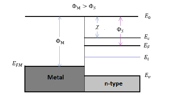
The electron affinity \(\chi\) and the metal work function \(\Phi_M\) are invariant fundamental properties that are remain unaffected by the contacting process. However, the work fuction of semiconductors is related with the electron affinity, the conduction band, and the Fermi energy:
\[\Phi_S = \chi + (E_c - E_F)_{FB} \label{1} \]
where
\[\chi = (E_0 -E_F) \label{2} \]
However, the situations in Figure 1 are not in equilibrium condition, since the Fermi energy in the metal is not aligned with the Fermi energy in semiconductor ( \(E_{FS} \neq E_{FM} \)). Therefore, electrons will keep transferring between the semiconductor and the metal until the \(E_F\) is aligned, which would cause a formation of depletion region between the MS contact. With different characteristics of the metal-semiconductor interface, two types of MS contact will be formed: the rectifying Schottky barrier contact and the Ohmic contact.
Schottky Barrier Contact
The Schottky barrier contact refers to the MS contact having a large potential barrier height formed when the Fermi energy of the metal and the semiconductor are aligned together. The barrier height \(\Phi_B\) is defined as the energy difference between the band edge with majority carriers and the Fermi energy of the metal. Since the Schottky barriers could lead to rectifying characteristics, it is normally used as a diode, which is a single MS junction with rectifying characteristics. Both n-type and p-type semiconductors can formed the Schottky contact, such as Titanium Silicide, and Platinum Silicide.
Under Equilibrium Condition (applied bias V=0)
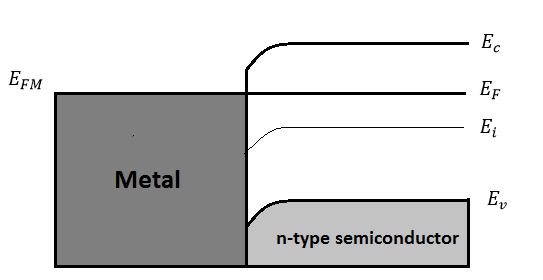
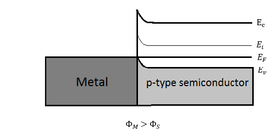
Consider the case of \(\Phi_M > \Phi_S \), electrons will transfer from the semiconductor to the metal due to their greater energy until the equilibrium condition is established. The net loss of electrons creates a negative charge in the metal and a positive charge in the semiconductor, which results a depletion region and a growing barrier at the semiconductor surface. As the result, the equilibrium band structure for a metal and a n-type semiconductor is illustrated in Figure 2.
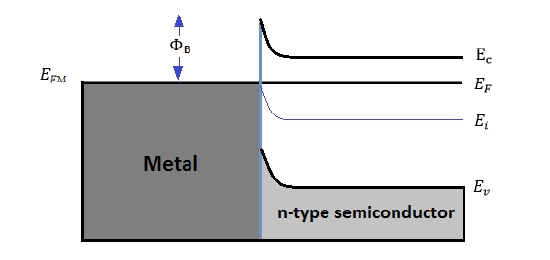
The surface potential-energy barrier \(\Phi_B\), the primary characteristics of the Schottky barrier, is characterized by the Schottky barrier height, which is a function of the metal and the semiconductor:
\[\Phi_B = \Phi_M - \chi , \quad \text {for n-type semiconductor} \label{3} \]
\[\Phi_B = {E_g \over q} + \chi - \Phi_M, \quad \text {for p-type semiconductor} \label {4} \]
The barrier results a high resistance when there is even a small applied voltage. Since the potential barrier height could be governed by the voltage bias, which has a significant influence of the electrical current flowing through the barrier, the effect of forward bias and reverse bias are interested.
Effect of Biasing
Consider the \(\Phi_M > \Phi_S \) MS contact, an current \(I\) will be formed if there is an applied biasing \(V_A\) on the metal and the semiconductor is connected to be grounded. (Figure 3) The current is defined to be positive when it flows from the metal to the semiconductor.

Forward Biasing
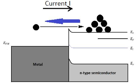
Under a forward biasing ( \(V_A > 0\)), the operation of MS junction is illustrated in Figure 4. The Fermi energy of metal becomes lower than the Fermi energy in the semiconductor \(E_F\), which results a reduction of the potential barrier \(\Phi_B\) across the semiconductor. Consequently, it will be much easier for electrons to pass over the barrier, which makes the electrons diffuse much easier from semiconductor to the metal. Therefore, as the \(V_A\)increasing, the current will increase rapidly, since more electrons will be able to overcome the surface barrier without coming back corresponds to the opposite direction of the current. There will be more electrons diffuse from the semiconductor towards the metal than the electrons drifting into the semiconductor, a positive current will be generated across the MS junction.
Reverse Biasing
With an negative applied bias on the metal (\(V_A < 0\)), the operation of MS junction is illustrated in Figure 5. The Fermi energy of metal becomes higher than the Fermi energy in the semiconductor, which results an increasing of the barrier potential across the MS junction. The large barrier will block the diffusion of electrons from semiconductor to the metal. Under a small reversed bias, only a small amount of electrons in the metal may be able to overcome the potential barrier. Therefore, the current \(I\) will become a small constant at reversed bias, which is characterized as the rectifying behavior.

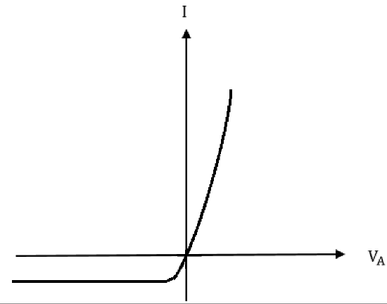
\(I-V\) Characteristics
In general, the current flowing through the Schottky contact can be defined with the applied voltage, which is very similar to those of pn-junction diode. The \(IV\) expression is:
\(I=I_0(e^{qV_A/kT}-1), \quad \text {where}\) \(I_0\) is a saturate current \(\label{5}\)
Under a forward bias (\(V_A>0\)), when the forward bias exceeds than a few \(kT/q\) volts, the current will be dominated by the exponential term. For the reverse bias (\(V_A<0\)), when the reverse bias greater than a few \(kT/q\) volts, the exponential term will be neglected, which results a small saturate current: \(I=-I_0\).The \(I-V\) characteristics is shown in Figure 6.
Ohmic Contact
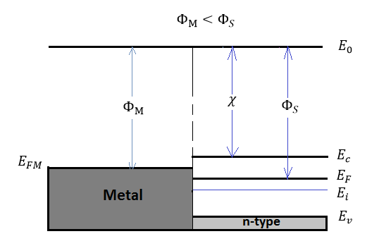
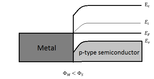
Not all MS contact can perform as the rectifying Schottky diode, since there is no potential barrier formed. Under this situation, when the current can be conducted in both directions of the MS contact, the contact is defined as the Ohmic contact. An ideal Ohmic contact is a low resistance, and non-rectifying junction with no potential exists between the the metal-semiconductor interface. Consider the case in Figure 1 (b), the MS contact with \(\Phi_M < \Phi_S \), electrons will transfer from the metal to the semiconductor due to their low energy, which will cause the Fermi level in semiconductor move up until the equilibrium state is established. The band diagram under equilibrium state is illustrated in Figure 7(a).
(a) (b)
Figure 7. (a) Energy band diagram under equilibrium for \(\Phi_M < \Phi_S \) and (b) Schematic \(IV\) characteristics of Ohmic contact
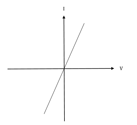
Since there is no barrier structure for electron flow from the semiconductor to metal, even a very small forward bias voltage (\(V_A > 0\)) will rise a large forward bias current. When there is an applied reverse bias voltage, a small potential barrier is formed for electron flow from metal to semiconductor. However, the small barrier will eventually vanish when the reverse bias voltage becomes larger. Consequently, there is a large reverse current flow when \(V < 0\). The \(I-V\) characteristic is shown in Figure 7(b).
Different with the rectifying Schottky contact, the Ohmic contact behaves a linear \(I-V\) curve that follows the Ohm's Law in both forward and reverse bias condition.
Conclusion
Overall, for a metal and an n-type semiconductor, a rectifying Schottky contact is formed when \(\Phi_M > \Phi_S \), and an Ohmic contact is formed when \(\Phi_M < \Phi_S \). Similarly, for a metal and an p-type semiconductor, the MS contact will be rectifying Schottky when \(\Phi_M < \Phi_S \), and Ohmic contact when \(\Phi_M > \Phi_S \). The summarization for the contact types is indicated in Table 1.
| n-type semiconductor | p-type semiconductor | |
|---|---|---|
| \(\Phi_M > \Phi_S \) | Rectifying | Ohmic |
| \(\Phi_M < \Phi_S \) | Ohmic | Rectifying |
Questions
1. Show the equilibrium energy band diagram for a metal to an p-type semiconductor where (a) \(\Phi_M < \Phi_S \) and (b) \(\Phi_M < \Phi_S \)
2. Find the expression of the barrier height \(\Phi_B\) of the rectifying p-type contact
3. When a MS contact is formed for \(\Phi_M = \chi\), under what conditions will the contact behaves as the Ohmic contact, and under what conditions will the contact behaves as the rectifying?
Answers
1. (a) For metal and p-type semiconductor, the equilibrium energy band diagrams are shown below:
2. Since \(\quad E_c - E_{FM} = \Phi_M - \chi\), it follows that
\(\Phi_B = E_{FM} - E_{v(interface)} = (E_c -E_v) - (E_{c(interface)} = E_{FM}\).
Therefore, \(\Phi_B = E_G + \chi - \Phi_M \quad \text {for an ideal p-type MS contact} \)
3. If \(\Phi_M = \chi \) in an ideal MS contact, the formation of contact types will be independent with the type of semiconductor doping.
References
1. Robert F. Pierret, Semiconductor Device Fundamentals, Second Edition. Chapter 14, pages 477-491.
2. John Wiley & Sons, Sze, S.M., Physics of Semiconductor Devices
Contributors and Attributions
- Sherry Cui (University of California, Davis, Materials Science and Engineering)