
Extrinsic Semiconductors
- Page ID
- 360
\( \newcommand{\vecs}[1]{\overset { \scriptstyle \rightharpoonup} {\mathbf{#1}} } \)
\( \newcommand{\vecd}[1]{\overset{-\!-\!\rightharpoonup}{\vphantom{a}\smash {#1}}} \)
\( \newcommand{\dsum}{\displaystyle\sum\limits} \)
\( \newcommand{\dint}{\displaystyle\int\limits} \)
\( \newcommand{\dlim}{\displaystyle\lim\limits} \)
\( \newcommand{\id}{\mathrm{id}}\) \( \newcommand{\Span}{\mathrm{span}}\)
( \newcommand{\kernel}{\mathrm{null}\,}\) \( \newcommand{\range}{\mathrm{range}\,}\)
\( \newcommand{\RealPart}{\mathrm{Re}}\) \( \newcommand{\ImaginaryPart}{\mathrm{Im}}\)
\( \newcommand{\Argument}{\mathrm{Arg}}\) \( \newcommand{\norm}[1]{\| #1 \|}\)
\( \newcommand{\inner}[2]{\langle #1, #2 \rangle}\)
\( \newcommand{\Span}{\mathrm{span}}\)
\( \newcommand{\id}{\mathrm{id}}\)
\( \newcommand{\Span}{\mathrm{span}}\)
\( \newcommand{\kernel}{\mathrm{null}\,}\)
\( \newcommand{\range}{\mathrm{range}\,}\)
\( \newcommand{\RealPart}{\mathrm{Re}}\)
\( \newcommand{\ImaginaryPart}{\mathrm{Im}}\)
\( \newcommand{\Argument}{\mathrm{Arg}}\)
\( \newcommand{\norm}[1]{\| #1 \|}\)
\( \newcommand{\inner}[2]{\langle #1, #2 \rangle}\)
\( \newcommand{\Span}{\mathrm{span}}\) \( \newcommand{\AA}{\unicode[.8,0]{x212B}}\)
\( \newcommand{\vectorA}[1]{\vec{#1}} % arrow\)
\( \newcommand{\vectorAt}[1]{\vec{\text{#1}}} % arrow\)
\( \newcommand{\vectorB}[1]{\overset { \scriptstyle \rightharpoonup} {\mathbf{#1}} } \)
\( \newcommand{\vectorC}[1]{\textbf{#1}} \)
\( \newcommand{\vectorD}[1]{\overrightarrow{#1}} \)
\( \newcommand{\vectorDt}[1]{\overrightarrow{\text{#1}}} \)
\( \newcommand{\vectE}[1]{\overset{-\!-\!\rightharpoonup}{\vphantom{a}\smash{\mathbf {#1}}}} \)
\( \newcommand{\vecs}[1]{\overset { \scriptstyle \rightharpoonup} {\mathbf{#1}} } \)
\(\newcommand{\longvect}{\overrightarrow}\)
\( \newcommand{\vecd}[1]{\overset{-\!-\!\rightharpoonup}{\vphantom{a}\smash {#1}}} \)
\(\newcommand{\avec}{\mathbf a}\) \(\newcommand{\bvec}{\mathbf b}\) \(\newcommand{\cvec}{\mathbf c}\) \(\newcommand{\dvec}{\mathbf d}\) \(\newcommand{\dtil}{\widetilde{\mathbf d}}\) \(\newcommand{\evec}{\mathbf e}\) \(\newcommand{\fvec}{\mathbf f}\) \(\newcommand{\nvec}{\mathbf n}\) \(\newcommand{\pvec}{\mathbf p}\) \(\newcommand{\qvec}{\mathbf q}\) \(\newcommand{\svec}{\mathbf s}\) \(\newcommand{\tvec}{\mathbf t}\) \(\newcommand{\uvec}{\mathbf u}\) \(\newcommand{\vvec}{\mathbf v}\) \(\newcommand{\wvec}{\mathbf w}\) \(\newcommand{\xvec}{\mathbf x}\) \(\newcommand{\yvec}{\mathbf y}\) \(\newcommand{\zvec}{\mathbf z}\) \(\newcommand{\rvec}{\mathbf r}\) \(\newcommand{\mvec}{\mathbf m}\) \(\newcommand{\zerovec}{\mathbf 0}\) \(\newcommand{\onevec}{\mathbf 1}\) \(\newcommand{\real}{\mathbb R}\) \(\newcommand{\twovec}[2]{\left[\begin{array}{r}#1 \\ #2 \end{array}\right]}\) \(\newcommand{\ctwovec}[2]{\left[\begin{array}{c}#1 \\ #2 \end{array}\right]}\) \(\newcommand{\threevec}[3]{\left[\begin{array}{r}#1 \\ #2 \\ #3 \end{array}\right]}\) \(\newcommand{\cthreevec}[3]{\left[\begin{array}{c}#1 \\ #2 \\ #3 \end{array}\right]}\) \(\newcommand{\fourvec}[4]{\left[\begin{array}{r}#1 \\ #2 \\ #3 \\ #4 \end{array}\right]}\) \(\newcommand{\cfourvec}[4]{\left[\begin{array}{c}#1 \\ #2 \\ #3 \\ #4 \end{array}\right]}\) \(\newcommand{\fivevec}[5]{\left[\begin{array}{r}#1 \\ #2 \\ #3 \\ #4 \\ #5 \\ \end{array}\right]}\) \(\newcommand{\cfivevec}[5]{\left[\begin{array}{c}#1 \\ #2 \\ #3 \\ #4 \\ #5 \\ \end{array}\right]}\) \(\newcommand{\mattwo}[4]{\left[\begin{array}{rr}#1 \amp #2 \\ #3 \amp #4 \\ \end{array}\right]}\) \(\newcommand{\laspan}[1]{\text{Span}\{#1\}}\) \(\newcommand{\bcal}{\cal B}\) \(\newcommand{\ccal}{\cal C}\) \(\newcommand{\scal}{\cal S}\) \(\newcommand{\wcal}{\cal W}\) \(\newcommand{\ecal}{\cal E}\) \(\newcommand{\coords}[2]{\left\{#1\right\}_{#2}}\) \(\newcommand{\gray}[1]{\color{gray}{#1}}\) \(\newcommand{\lgray}[1]{\color{lightgray}{#1}}\) \(\newcommand{\rank}{\operatorname{rank}}\) \(\newcommand{\row}{\text{Row}}\) \(\newcommand{\col}{\text{Col}}\) \(\renewcommand{\row}{\text{Row}}\) \(\newcommand{\nul}{\text{Nul}}\) \(\newcommand{\var}{\text{Var}}\) \(\newcommand{\corr}{\text{corr}}\) \(\newcommand{\len}[1]{\left|#1\right|}\) \(\newcommand{\bbar}{\overline{\bvec}}\) \(\newcommand{\bhat}{\widehat{\bvec}}\) \(\newcommand{\bperp}{\bvec^\perp}\) \(\newcommand{\xhat}{\widehat{\xvec}}\) \(\newcommand{\vhat}{\widehat{\vvec}}\) \(\newcommand{\uhat}{\widehat{\uvec}}\) \(\newcommand{\what}{\widehat{\wvec}}\) \(\newcommand{\Sighat}{\widehat{\Sigma}}\) \(\newcommand{\lt}{<}\) \(\newcommand{\gt}{>}\) \(\newcommand{\amp}{&}\) \(\definecolor{fillinmathshade}{gray}{0.9}\)Semiconductors are materials that possess the unique ability to control the flow of their charge carriers, making them valuable in applications like cell phones, computers, and TVs. An extrinsic semiconductor is a material with impurities introduced into its crystal lattice. The goal of these impurities is to change the electrical properties of the material, specifically (increasing) its conductivity. Today, extrinsic semiconductors are a part of innovative, modern technology devices (including efficient solid state lighting and renewable energy) such as light emitting diodes, solar cells, lasers, and transistors.
Introduction
Extrinsic semiconductors are just intrinsic semiconductors that have been doped with impurity atoms (one dimensional substitutional defects in this case). Doping is the process where semiconductors increase their electrical conductivity by introducing atoms of different elements into their lattice. A semiconductor can be doped by vapor phase epitaxy, where some concentration of impurities in their gaseous phase is contacted with the semiconductor wafer, or by being grown in with the wafer itself with the help of photolithography (microprocessing areas of a wafer), diffusion (gradient controlled particle motion), and ion implantation (utilizing an electric field to contact an ion with a solid) to increase the dopant concentration in certain parts of the wafer. Based on whether the added impurities are electron donors or acceptors, the semiconductor's Fermi level (the energy state below which all allowable energy states are filled and above which all states are empty as the temperature approaches 0 Kelvin) is able to move either up or down from its original position in the center of the energy band gap (the gap between the valence and conduction bands of the semiconductor).
If a semiconducting material is doped with atoms that can donate electrons, it is known as an n-type semiconductor which uses those donated electrons to increase its conductivity. If it is doped with with atoms that can accept electrons, it is known as a p-type semiconductor which uses the lack of electrons in the lattice, called holes (can be considered as positive charges as well), to increase its conductivity as well. Aside from being dependent on the concentration of dopants, both n-type and p-type semiconductors are dependent on temperature changes, especially their electrical conductivities, carrier mobilities (how freely a charge carrier can move), and even the Fermi levels. The mobilities are based off of two different temperature dependent scattering effects, called lattice scattering and ionized impurity scattering. Lattice scattering, dominant at higher temperatures, is based on the thermal vibrations of the semiconductor atoms which act as obstacles to mobile charge carriers. Ionized impurity scattering, dominant at lower temperatures, depends on the number of dopant ions, which all behave as scattering centers, and their ability to negate charge carriers from being moving to different energy levels because of the electrostatic attraction between ion and carrier known as Coulomb's Law, described as
\[F = \dfrac{qQ}{4\pi\epsilon_0 r^2} \label{1}\]
where q and Q are the charges (opposite charges) on the charge carrier and dopant ion, \(\epsilon_0\) is the permittivity of free space, r is the distance between ion and carrier, and F is the electrostatic attractive force that each of them experience.
No matter what happens with doping, however, the one equation that always remains true for extrinsic semiconductors is
\[np = n_i ^2 \label{2}\]
where n is the electron concentration, p is the hole concentration, and\(n_i\) is the intrinsic carrier concentration (the concentration had the semiconductor not been doped).
N-type Semiconductors
An n-type semiconductor is one that has donor dopants deposited into its crystal lattice. Here, electrons are called the majority carriers and holes are the minority carriers. One of the most common examples of this is Silicon or Germanium, from group IV in the periodic table, being doped with Phosphorus or Arsenic atoms (from group V), both of which has one extra valence electron per atom. The dopant atom is able to enter the lattice, substitute in for one Si atom while bound to four others (a covalent bond), and release its extra, loosely bounded valence electron into the Si lattice.
As stated before, the primary reason to inject the semiconducting wafer with impurities is to increase its conductivity, found to be
\[\sigma = q\mu_n n(T) + q\mu_p p(T) \label{1}\]
where q is the charge of an electron (~ 1.6 *10^-19 Coulombs), \(\mu_n\) and \(\mu_p\) are the electron and hole mobilities respectively, and n(T) and p(T) are the concentrations of electrons in the conduction band or holes in the valence band. Both the mobilities and the two concentration variables are temperature dependent, however for right now consider the temperature as constant at around room temperature. For all practical purposes in an n-type semiconductor at room temperature, the conductivity term from the hole concentration is negligible because usually, \(N_D\) >> \(n_i\) where \(N_D\) is the concentration of donor dopants, all of whose electrons are in the conduction band at 300 K, and \(n_i\) is the intrinsic carrier concentration of the semiconductor. If the donor electron concentration is much greater than the intrinsic carrier concentration, then the hole concentration contributing to the conductivity is even smaller at \(\dfrac{n_i ^2}{N_D}\), allowing it to be neglected.
Once inserted into the semiconductor, the donor dopants are able to form a donor level in the band gap near the conduction band, previously where there were no existing states, because it is now energetically favorable to do so. This means that the donated electrons will require a much smaller increase in energy to be excited into the conduction band, where the free flowing electrons can increase conductivity. Therefore, as doping increases, the conductivity of an n-type semiconductor increases as well (more donor states means more donated free electrons that can be promoted into the conduction band).
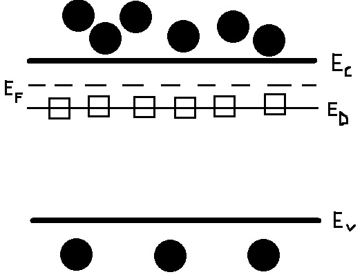
Figure \(\PageIndex{1}\) displays the behavior of the donor doped semiconductor at room temperature. Ec represents the conduction band, Ev is the valence band, \(E_D\) shows the donor level (containing the immobile donor ions), and \(E_F\) is the Fermi level. The black circles are electrons, while the white squares represent the empty, immobile donor states (because all the donor electrons are able to be promoted into the conduction band at room temperature) that do not affect the conductivity. The electrons below Ev are shown, only to point out that there are still many intrinsic carriers in the valence band that are still yet to be promoted to the conduction band (a minimal amount of intrinsic have been promoted from the valence band so far, though). There is a minimal hole concentration in the valence band but this has not been shown in figure 1, mainly to illustrate the greater importance of electrons in n-type semiconductors. Considering that the Fermi level is defined as the states below which all allowable energy states are filled and all states above are empty at the temperature approaches 0 Kelvin, it makes sense that \(E_F\) would increase from from its middle of the band gap intrinsic position because of the donor level near the conduction band (filled states are those that are occupied by electrons). Another way to think about this is that the majority of the density of energy states should be contained underneath the Fermi level (at 0 Kelvin, the Fermi level is at the middle of the band gap but the donor dopants are not considered as energy states yet, since all motion ceases). Looking at the equation for Fermi level (ignoring temperature dependence for now since it is constant) confirms this, as \[E_F = kTln(\dfrac{N_D}{n_i}) - E_i\]. where \(E_i\) is the is the energy level in the middle of the band gap. With everything else constant, increasing the donor concentration increases the Fermi level, meaning that electrons can more easily reach the conduction band.
From this point, the most important calculation (other than conductivity) that can lead to building efficient devices with multiple applications is to find the concentration of electrons in the conduction band. At room temperature, this concentration is simply \(N_D\) but in general, it is \[N_C e^\dfrac{E_F - E_C}{kT}\] where \(N_C\) is the density of energy states in the conduction band and k is the Boltzmann constant (1.38 * 10^ -23 Joules/(degree Kelvin)). \(N_C\) can be further simplified as
\[2[\dfrac{2\pi m_e ^* kT}{h^2}]^\dfrac{3}{2} \label{2}\]
where \(m_e ^*\) is the effective mass of an electron and h is Planck's constant (6.626 * 10^-34 J*seconds).
P-type Semiconductors
A p-type semiconductor is one that has acceptor dopants deposited into its crystal lattice. Here, holes are called the majority carriers and electrons are the minority carriers. One of the most common examples of this is Silicon or Germanium, from group IV in the periodic table, being doped with Boron or Gallium atoms (from group III), both of which has one fewer valence electron per atom. The dopant atom is able to enter the lattice, substitute in for one Si atom while bound to four others, and accept an electron from an adjacent atom into its covalent bond,. This is how the lack of an electron, or hole, moves through the valence band of the material, making it conductive (the same process of replacing a hole with an electron, moving the hole to another location in the lattice keeps repeating).
As mentioned earlier, the primary reason to inject the semiconducting wafer with impurities is to increase its conductivity, which is
\[\sigma = q\mu_n n(T) + q\mu_p p(T) \label{3}\]
where q is the charge of an electron, \(\mu_n\) and \(\mu_p\) are the electron and hole mobilities respectively, and n(T) and p(T) are the concentrations of electrons in the conduction band or holes in the valence band. Both the mobilities and the two concentration variables are temperature dependent, however for right now consider the temperature as constant at around room temperature. For all practical purposes in a p-type semiconductor at room temperature, the conductivity term from the electron concentration is negligible because usually, \(N_A\) >> \(n_i\) where \(N_A\) is the concentration of acceptor dopants, all of whose holes are in the valence band by 300 K, and \(n_i\) is the intrinsic carrier concentration of the semiconductor. If the hole concentration is much greater than the intrinsic carrier concentration, then the electron concentration contributing to the conductivity is even smaller at \(\dfrac{n_i ^2}{N_A}\), allowing it to be neglected.
Once inserted into the semiconductor, the acceptor dopants are able to form an acceptor level in the band gap near the valence band, previously where there were no existing states, because it is now energetically favorable to do so. This means that the electrons in the valence band can be excited into this acceptor level in the band gap (as opposed to the conduction band) to complete the covalent bond. This process leaves behind free holes that are able to propagate through the valence band, where they can increase the conductivity. Therefore, as doping increases, the conductivity of a p-type semiconductor also increases (more acceptor states means more free holes that can permeate the valence band).
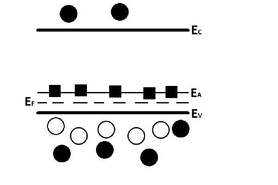
Figure 2 displays the behavior of the acceptor doped semiconductor at room temperature. Ec represents the conduction band, Ev is the valence band, \(E_A\) shows the acceptor level (containing the immobile acceptor ions), and \(E_F\) is the Fermi level. The black circles are electrons, while the black squares represent the empty (electron rich but devoid of holes), immobile acceptor states (because all the acceptor ions' holes are able to pervade the valence band at room temperature) that do not affect the conductivity. The white circles are the holes that that have formed due to the acceptor dopants requiring electrons to complete their covalent bonding. There are more holes than electrons in the valence band in the picture because holes are the majority carriers. The electrons above Ev are shown, only to point out that there are carriers that that exist in the conduction band that have been promoted from the valence band (a minimal amount have been promoted from the valence band, though). Considering that the Fermi level is defined as the states below which all allowable energy states are filled and all states above are empty at the temperature approaches 0 Kelvin, it makes sense that \(E_F\) would decrease from from its middle of the band gap intrinsic position because of the acceptor level near the valence band ("filled" states are occupied by electrons). Another way to think about this is that the majority of the density of energy states should be contained underneath the Fermi level (at 0 Kelvin, the Fermi level is at the middle of the band gap and the acceptor dopants are not considered as energy states anyways since all motion ceases and there are no mobile electrons present yet, only holes) The downward shift of the Fermi level highlights the fact that p-type semiconductors emphasizes conduction of holes in the valence band as opposed to conduction of electrons in the conduction band, which means that the number of electrons above \(E_F\) are at a minimum. Looking at the equation for Fermi level (ignoring temperature dependence for now since it is constant) confirms this, as
\[E_F = -kT\ ln \left(\dfrac{N_D}{n_i} \right) + E_i. \label{4}\]
where \(E_i\) is the is the energy level in the middle of the band gap. With everything else constant, increasing the acceptor concentration decreases the Fermi level, meaning that holes can more easily reach the valence band.
From this point, the most important calculation (other than conductivity) that can lead to creating innovative, versatile devices is to find the concentration of holes in the valence band. At room temperature, this concentration is simply \(N_A\) but in general, it is
\[N_V e^\dfrac{E_V - E_F}{kT} \label{5}\]
where \(N_V\) is the density of energy states in the valence band and k is the Boltzmann constant. \(N_C\) can be further simplified as \[2[\dfrac{2\pi m_h^* kT}{h^2}]^\dfrac{3}{2}\] where \(m_h ^*\) is the effective mass of a hole and h is Planck's constant.
Temperature Dependence
Before exploring the temperature dependence of electrical conductivities, carrier mobilities (with lattice and ionized impurity scattering), and Fermi levels, the doping dependence of ionized impurity scattering needs to be considered.
In general, scattering decreases electron mobility of charge carriers by acting as obstacles. In other words, charge carriers are not able to flow easily throughout the material. Ionized impurity scattering occurs when there are many donor or acceptor dopants present in the lattice. As doping increases, each added donor or acceptor level can be thought of as an additional "scattering center" added to the lattice, another obstacle that can impede charge carrier motion. This type of scattering does not depend on any sort of thermal vibration, but rather takes advantage of the fact that carriers do not have enough energy to move to any different energy levels. This means that for n-type semiconductors, the ionized donor atoms, positive ions, are able to cause an electrostatic attraction with the donated electrons while in p-type semiconductors, the ionized acceptor atoms (negative ions) cause an electrostatic attraction with the holes created in the lattice. Carrier Energy barriers are not an issue when thermal energy is a major factor. This means that for both n and p-type conductors, ionized impurity scattering is dominant at lower temperatures and its effects gradually decrease as the temperature increases.
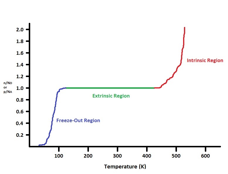
Figure 3 clearly demonstrates the phases an extrinsic semiconductor's majority carrier goes through while being heated up while holding the amount of dopants constant. For an n-type semiconductor, the beginning of the Freeze-Out Region represents the area where the donor ions are situated at the donor level, but the free electrons are unable to move due to the 0 Kelvin temperature. As the temperature increases in the blue regime, a few of the donor electrons get excited into the conduction band while others are still impeded due to the ionized impurity scattering, which decreases the overall mobility of the electrons. As the temperature starts increasing toward the Extrinsic Region, the effect of ionized impurity scattering slowly fades away, increasing the electron mobility, and the amount of electrons being promoted from the donor level to the conduction band increases even more. At this point, a minimal amount of the intrinsic electrons are promoted from the valence band (however this is still considered as a negligible effect). Since conductivity directly depends on electron mobility and the concentration of electrons in the conduction band, which increases with increasing temperature according to the equation near the end of the N-Type Semiconductor section, the conductivity also increases. Throughout the green regime, all the donor level electrons are excited into the conduction band and neither scattering effect is prominent, which means that the conductivity increases even more. Meanwhile, a few more intrinsic electrons from the valence band are promoted into the conduction band, yet this is still negligible compared to the concentration of donated electrons already in or above \(E_V\). As the temperature proceeds into the Intrinsic Region, intrinsic electrons from the valence band are excited into the conduction band at a faster rate (leaving behind an equivalent amount of holes in the valence band) and the conductivity continues to increase. However, this is when the lattice scattering mechanism is activated. This means that the semiconductors atoms in the lattice undergo thermal vibrations, which act as obstacles to the moving electrons, causing the mobility to decrease (since the electron concentration is more important, conductivity still increases even as mobility begins to decrease). Throughout the red regime, the electrons from the valence band are promoted into the conduction band and create holes in the valence band. As this continues, the n-type semiconductor essentially becomes an intrinsic semiconductor, with all the intrinsic electrons now in the conduction band and the equivalent amount of holes left behind in the valence band. Lattice scattering is at its greatest due to the thermal vibrations, meaning that the electron mobility decreases even further. However, conductivity is at its greatest because even though the electrons have a harder time moving through the material, there are so many more of them at higher temperatures.
In this entire process, the most complex concept to understand is the Fermi level, which is best decribed in words and not equations for temperature changes. In the beginning blue region, the Fermi level is still at the middle of the band gap because all motion stops and there are no densities of states that even exist. Through the blue region towards the point where the material acts like an n-type semiconductor, the Fermi level moves up to a point where the majority of the states are contained underneath it (Fermi level between conduction band and donor level). However, as more intrinsic electrons start adding to the conductivity in the red regime of the figure, the Fermi level starts moving down closer to the middle of the band gap resembling an intrinsic semiconductor.
For p-type semiconductors, the conductivity and mobility trends follow those of the n-type semiconductor along figure 3. As temperature increases, ionized impurity scattering effects decrease (increasing mobility) because holes gain enough energy to move towards the valence band and electrons from the valence band occupy the acceptor states to complete the covalent bonds, which increases the holes' conductivity. The hole mobility increases even more at the Extrinsic Region because ionized impurity scattering fades away and lattice scattering has not been activated yet. Meanwhile, all the acceptor states are devoid of holes, which means that the conductivity throughout the valence band increases even more. At this point, there are a few intrinsic electrons (still a negligible effect) that are excited into the conduction band. As the temperature increases into the Intrinsic Region, more intrinsic electrons are promoted into the conduction band, but yet again the lattice scattering mechanism is activated, where the semiconductor atoms begin the vibrate due to increased thermal energy, this impeded the motion of all the charge carriers, causing both mobilities to decrease. However, since conductivity is more heavily determined by the carrier concentrations (which increase with increasing temperature) it continues to increase. Through the red regime, more intrinsic electrons in the valence band get excited into the conduction band at a faster rate, leaving behind more holes. As this continues, the p-type semiconductor gradually becomes an intrinsic semiconductor with all the intrinsic electrons that are promoted, leaving behind even more holes. The lattice scattering is at its highest point from all the thermal vibrations (electron and hole mobilities decrease even further). However, conductivity is at its maximum point because even though both charge carriers experience multiple scattering events, there are so many more holes and electrons that conduct in their respective bands at higher temperatures.
Again through this process, the most complex concept to understand is the Fermi level, (best decribed verbally and not mathematically for temperature changes). In the beginning blue region, the Fermi level is still at the middle of the band gap because all motion stops and there are no densities of states that even exist. Through the blue region towards the point where the material acts like an p-type semiconductor, the Fermi level moves down to a point where the majority of the states are contained underneath it (Fermi level between valence band and acceptor level). However, as more intrinsic electrons start adding to the conductivity in the red regime of the figure, the Fermi level starts moving up closer to the middle of the band gap resembling an intrinsic semiconductor.
Questions
- What is the primary difference between an n-type and a p-type semiconductor?
- Name and describe the difference between the two different types of scattering events.
- What are the three temperature dependent regions/behaviors for an extrinsic semiconductor?
Answers
- An n-type semiconductor has been doped with impurity atoms that contains one more electron per atom, allowing them to donate electrons which can conduct in the conduction band. A p-type semiconductor has been doped with impurity atoms that contain one fewer electron per atom, letting them accept electrons and conduct a "lack" of electrons, or holes, in the valence band.
- Lattice scattering occurs at higher temperatures because it deals with activating thermal vibrations that impede charge carrier motion which decreases the overall carrier mobility. As temperature decreases, thermal vibrations are reduced and lattice scattering loses its effect. Lattice scattering has no measurable doping dependence. Ionized impurity scattering occurs at low temperatures and increases with increasing dopants. This type of scattering mechanism takes advantage of the fact that at low temperatures, carriers do not have enough energy to move to any different energy levels, meaning that the ionized dopant ions cause an electrostatic attraction with electrons or holes in an n-type or p-type semiconductor respectively. Increasing the number of dopants adds to the number of "scattering centers" in a semiconducting material, meaning more obstacles that can limit the movement of charge carriers.
- The three regions/behaviors are the: Freeze-Out Region, Extrinsic Region, and Intrinsic Region.
Additional Links
- Diffusion (Wikipedia)
- Band Theory of Semiconductors
- Extrinsic Semiconductor (Wikipedia)
- How Semiconductors Work
- Photolithography (Wikipedia)
- Bands For Doped Semiconductors (HyperPhysics)
- Ion Implantation (Wikipedia)
- Doping (Wikipedia)
References
- R Pierret. (1996). Semiconductor Device Fundamentals. Reading, Mass.: Addison-Wesley, 1996. 29-38. Print.
- R Hummel. (2012). Electronic Properties of Materials (4th ed.). New York, NY: Springer, 2012. Print.
- S Kasap and P Capper. (2007). Springer Handbook of Electronic and Photonic Materials (4th ed.).
Contributors and Attributions
- Niteesh Marathe (University of California, Davis Class of 2015)