
Intrinsic Semiconductors
- Page ID
- 362
\( \newcommand{\vecs}[1]{\overset { \scriptstyle \rightharpoonup} {\mathbf{#1}} } \)
\( \newcommand{\vecd}[1]{\overset{-\!-\!\rightharpoonup}{\vphantom{a}\smash {#1}}} \)
\( \newcommand{\dsum}{\displaystyle\sum\limits} \)
\( \newcommand{\dint}{\displaystyle\int\limits} \)
\( \newcommand{\dlim}{\displaystyle\lim\limits} \)
\( \newcommand{\id}{\mathrm{id}}\) \( \newcommand{\Span}{\mathrm{span}}\)
( \newcommand{\kernel}{\mathrm{null}\,}\) \( \newcommand{\range}{\mathrm{range}\,}\)
\( \newcommand{\RealPart}{\mathrm{Re}}\) \( \newcommand{\ImaginaryPart}{\mathrm{Im}}\)
\( \newcommand{\Argument}{\mathrm{Arg}}\) \( \newcommand{\norm}[1]{\| #1 \|}\)
\( \newcommand{\inner}[2]{\langle #1, #2 \rangle}\)
\( \newcommand{\Span}{\mathrm{span}}\)
\( \newcommand{\id}{\mathrm{id}}\)
\( \newcommand{\Span}{\mathrm{span}}\)
\( \newcommand{\kernel}{\mathrm{null}\,}\)
\( \newcommand{\range}{\mathrm{range}\,}\)
\( \newcommand{\RealPart}{\mathrm{Re}}\)
\( \newcommand{\ImaginaryPart}{\mathrm{Im}}\)
\( \newcommand{\Argument}{\mathrm{Arg}}\)
\( \newcommand{\norm}[1]{\| #1 \|}\)
\( \newcommand{\inner}[2]{\langle #1, #2 \rangle}\)
\( \newcommand{\Span}{\mathrm{span}}\) \( \newcommand{\AA}{\unicode[.8,0]{x212B}}\)
\( \newcommand{\vectorA}[1]{\vec{#1}} % arrow\)
\( \newcommand{\vectorAt}[1]{\vec{\text{#1}}} % arrow\)
\( \newcommand{\vectorB}[1]{\overset { \scriptstyle \rightharpoonup} {\mathbf{#1}} } \)
\( \newcommand{\vectorC}[1]{\textbf{#1}} \)
\( \newcommand{\vectorD}[1]{\overrightarrow{#1}} \)
\( \newcommand{\vectorDt}[1]{\overrightarrow{\text{#1}}} \)
\( \newcommand{\vectE}[1]{\overset{-\!-\!\rightharpoonup}{\vphantom{a}\smash{\mathbf {#1}}}} \)
\( \newcommand{\vecs}[1]{\overset { \scriptstyle \rightharpoonup} {\mathbf{#1}} } \)
\(\newcommand{\longvect}{\overrightarrow}\)
\( \newcommand{\vecd}[1]{\overset{-\!-\!\rightharpoonup}{\vphantom{a}\smash {#1}}} \)
\(\newcommand{\avec}{\mathbf a}\) \(\newcommand{\bvec}{\mathbf b}\) \(\newcommand{\cvec}{\mathbf c}\) \(\newcommand{\dvec}{\mathbf d}\) \(\newcommand{\dtil}{\widetilde{\mathbf d}}\) \(\newcommand{\evec}{\mathbf e}\) \(\newcommand{\fvec}{\mathbf f}\) \(\newcommand{\nvec}{\mathbf n}\) \(\newcommand{\pvec}{\mathbf p}\) \(\newcommand{\qvec}{\mathbf q}\) \(\newcommand{\svec}{\mathbf s}\) \(\newcommand{\tvec}{\mathbf t}\) \(\newcommand{\uvec}{\mathbf u}\) \(\newcommand{\vvec}{\mathbf v}\) \(\newcommand{\wvec}{\mathbf w}\) \(\newcommand{\xvec}{\mathbf x}\) \(\newcommand{\yvec}{\mathbf y}\) \(\newcommand{\zvec}{\mathbf z}\) \(\newcommand{\rvec}{\mathbf r}\) \(\newcommand{\mvec}{\mathbf m}\) \(\newcommand{\zerovec}{\mathbf 0}\) \(\newcommand{\onevec}{\mathbf 1}\) \(\newcommand{\real}{\mathbb R}\) \(\newcommand{\twovec}[2]{\left[\begin{array}{r}#1 \\ #2 \end{array}\right]}\) \(\newcommand{\ctwovec}[2]{\left[\begin{array}{c}#1 \\ #2 \end{array}\right]}\) \(\newcommand{\threevec}[3]{\left[\begin{array}{r}#1 \\ #2 \\ #3 \end{array}\right]}\) \(\newcommand{\cthreevec}[3]{\left[\begin{array}{c}#1 \\ #2 \\ #3 \end{array}\right]}\) \(\newcommand{\fourvec}[4]{\left[\begin{array}{r}#1 \\ #2 \\ #3 \\ #4 \end{array}\right]}\) \(\newcommand{\cfourvec}[4]{\left[\begin{array}{c}#1 \\ #2 \\ #3 \\ #4 \end{array}\right]}\) \(\newcommand{\fivevec}[5]{\left[\begin{array}{r}#1 \\ #2 \\ #3 \\ #4 \\ #5 \\ \end{array}\right]}\) \(\newcommand{\cfivevec}[5]{\left[\begin{array}{c}#1 \\ #2 \\ #3 \\ #4 \\ #5 \\ \end{array}\right]}\) \(\newcommand{\mattwo}[4]{\left[\begin{array}{rr}#1 \amp #2 \\ #3 \amp #4 \\ \end{array}\right]}\) \(\newcommand{\laspan}[1]{\text{Span}\{#1\}}\) \(\newcommand{\bcal}{\cal B}\) \(\newcommand{\ccal}{\cal C}\) \(\newcommand{\scal}{\cal S}\) \(\newcommand{\wcal}{\cal W}\) \(\newcommand{\ecal}{\cal E}\) \(\newcommand{\coords}[2]{\left\{#1\right\}_{#2}}\) \(\newcommand{\gray}[1]{\color{gray}{#1}}\) \(\newcommand{\lgray}[1]{\color{lightgray}{#1}}\) \(\newcommand{\rank}{\operatorname{rank}}\) \(\newcommand{\row}{\text{Row}}\) \(\newcommand{\col}{\text{Col}}\) \(\renewcommand{\row}{\text{Row}}\) \(\newcommand{\nul}{\text{Nul}}\) \(\newcommand{\var}{\text{Var}}\) \(\newcommand{\corr}{\text{corr}}\) \(\newcommand{\len}[1]{\left|#1\right|}\) \(\newcommand{\bbar}{\overline{\bvec}}\) \(\newcommand{\bhat}{\widehat{\bvec}}\) \(\newcommand{\bperp}{\bvec^\perp}\) \(\newcommand{\xhat}{\widehat{\xvec}}\) \(\newcommand{\vhat}{\widehat{\vvec}}\) \(\newcommand{\uhat}{\widehat{\uvec}}\) \(\newcommand{\what}{\widehat{\wvec}}\) \(\newcommand{\Sighat}{\widehat{\Sigma}}\) \(\newcommand{\lt}{<}\) \(\newcommand{\gt}{>}\) \(\newcommand{\amp}{&}\) \(\definecolor{fillinmathshade}{gray}{0.9}\)Semiconductors are one of the three classes of electrical materials and are the foundation of every solid-state electronic device which is in use today. Intrinsic semiconductors, also known as pure or undoped semiconductors, describe perfect semiconductor crystals which are free from defects and impurities of other elements. Intrinsic semiconductors which are intentionally doped with other elements are referred to as Extrinsic Semiconductors. Intrinsic properties are found in all semiconductor materials, even those doped with other elements, with the doping elements introducing other desired properties.
Introduction
All semiconductors have intrinsic properties which are described here; even Extrinsic Semiconductors have base intrinsic properties. Intrinsic by definition means natural or inherent, and intrinsic semiconductors are the bulk properties of the semiconductor material itself, not those of dopants or impurities. Silicon and germanium are the two most commonly used examples of intrinsic semiconductors, as they are elemental semiconductors and were some of the first widely studied and used semiconductors. The electronic structure of semiconductors are the foundation of their unique properties. The mechanisms which make semiconductors their own class of material is based on the electrical structure, which dictates the core properties of semiconductors.
Electrical Structure
The properties of intrinsic semiconductors can be described using Band Theory of semiconductors, which is shown in Figure 1.
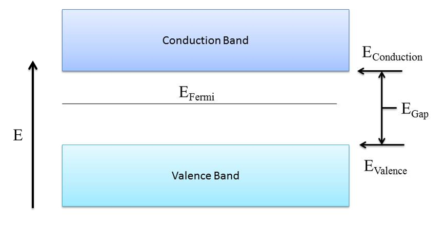
While the band structure of semiconductors may look very similar to that of an insulator, the band gap between the conduction and valence bands in a semiconductor is of much lower energy, typically less than 4eV. The properties of semiconductors are strongly dependent on temperature. This temperature dependence is because at 0K, there are no electrons in the conduction band. This is directly related to the Fermi energy, which is the maximum energy of an electron at 0K. Since the band gap, or forbidden region, has no probability of an electron occupying this region, the maximum energy an electron in a semiconductor can attain at 0 K is at the top edge of the valence band. As temperature increases, electrons in the valence band may gain enough energy to jump the band gap into the conduction band, and they leave behind a hole, which is an area of local positive charge the electron once occupied. The number of electrons crossing the gap is temperature dependent and depends on the specific intrinsic material. These electron hole pairs are attracted to each other by their electric charge and are called an exciton. In intrinsic semiconductors there is an equal number of electrons and holes in the material; for every electron to be promoted across the gap, there is a hole left behind. Band gap energy, which is dependent on the material, is also temperature dependent and decreases with temperature to a limited extent based on the material. The band gap energy Egap is related by \[E_{gap}=E_{gap_{O}}-\frac{-\xi T^{2}}{T+\Theta _{D}} Eq. 1 _{[2]}\] where EgapO is the band gap energy at 0K, ξ is a constant, T is the temperature, and θD is the Debye temperature which is material dependent.
The band gap energy and the number of electrons and holes in the valence and conduction bands, as well as a pure crystalline lattice, are important to the understanding of the electronic structure of intrinsic semiconductors, and are the basis for understanding the properties of semiconductors.
Purification/Processing
One of the most important issues related to intrinsic semiconductor properties are the lack of impurities within the material. Impurities can alter the band structure, band gap, Fermi energy, and electron and hole concentrations of a semiconductor, just as dopants do in Extrinsic Semiconductors. Thus, the purity of intrinsic semiconductor materials must be less than a few parts per billion [4], and can be purified beyond 99.999% [4] for specific applications.
Much of the purification of semiconductors is done via chemical processes, but processes such as zone refining are used on already solidified materials. Zone refining is a process where a solid piece of material is heated in a local spot at the end of the material until a small melted region has formed at the end, and slowly moved down the entire length of the material until all the material has experienced local melting. The reasoning behind this process is that the liquid melt can dissolve more impurities than the solid, and thus traps impurities in the melt instead of the solidified material. After the process has been completed, the end which contains the solidified melt is then cut off to remove the concentrated impurity region. The process can be repeated for further refinement, but more bulk material must be sacrificed.
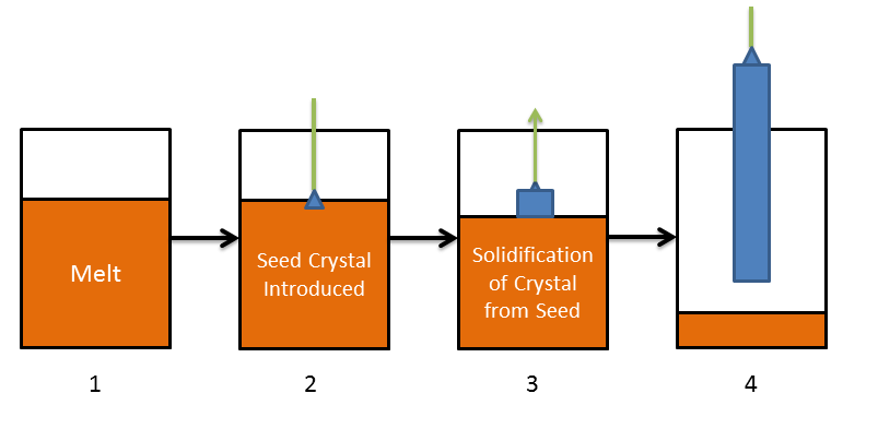
Formation of bulk semiconductors is accomplished by different methods, but the Czochralski process is typically used to create large single crystal ingots, or "boules" from which semiconductor wafers are produced. The Czochralski process, shown in Figure 2, consists of a melt of either high purity silicon or germanium in a crucible (Step 1) and a seed crystal. The seed crystal is characterized by crystalline lattice orientation beforehand and prepared so the crystal will form in the desired orientation. The seed crystal is then introduced into the melt (Step 2), and slowly pulled out and rotated as the melt solidifies around the seed crystal (Step 3). Controlling the melt temperature and rate of cooling of the solidified crystal which is formed from the seed crystal is vital to this process. The single crystal ingot is finally removed once most of the melt has been used (Step 4). This process is typically conducted in an inert environment, as to reduce the introduction of impurities into the crystal during formation.
Electrical Properties
Semiconductors, as mentioned before, are one of the three classes of electronic materials. Semiconductor materials, due to the band structure, become more conductive with an increase in temperature. This property is directly related to the concentration of electrons and holes in the conduction and valence bands, and this concentration of electrons and holes is directly related to temperature. The concentrations of electrons/holes in the conduction/valence band edge Ne/h are described by
\[N_{e/h}=2\left ( \dfrac{2\pi m_{e/h}^{*} k_{b} T}{h^{2}} \right )^{\frac{3}{2}}e^{\frac{-E_{gap}}{2k_{b}T}} \label{2}\]
which is a function of the effective mass of an electron/hole m*e/h, Boltzmann constant kB, temperature T, Planck's constant h, and the band gap energy Egap. The concentration is given in terms of number of carriers. Known data for silicon and Eq 2. was used to produce Figure 3, which is a representative example of electron and hole carriers in an intrinsic semiconductor in relation to temperature.

Figure 3 shows a sharp increase in carriers at around 600K. At lower temperatures, if there were impurities within the crystal that altered the electrons within the crystal, the additional impurities would alter the concentration of holes or electrons in the electronic structure. The importance of electrons and holes in the conduction and valence band is a direct link to conductivity. The conductivity σ of an intrinsic semiconductor is \[\sigma =e\mu_{e}N_{e}+e\mu_{h}N_{h} Eq. 3 _{[1][2]}\] and is based on the number of electron/hole carriers in the conduction/valence band Ne/h, the mobility of electrons/holes in the conduction/valence band μe/h, and the charge of an electron e.
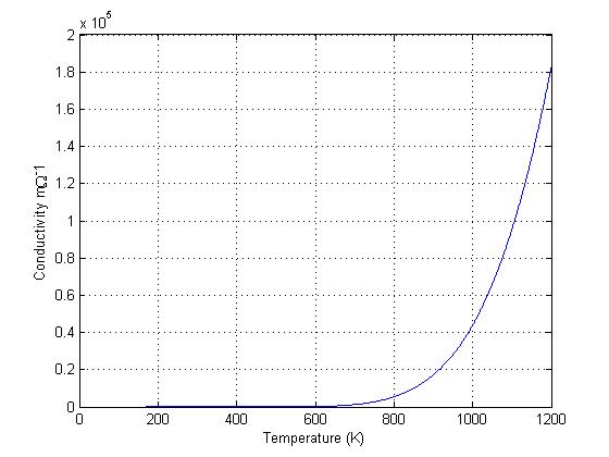
The conductivity of silicon, based on the carrier density data from Figure 3, was plotted using Eq 3 and shown in Figure 4. Notice the similarity between Figure 3 & 4, as the electrons and holes are the source of conductivity in intrinsic semiconductors. Figure 4 clearly shows the large rise in conductivity at high temperatures, just as there is a rise in carrier concentration in the same temperature region. This rise in conductivity with increased temperatures is opposite of Metals, as metals decrease in conductivity as temperature increases. This property makes semiconductors an option as a material for use in high temperature electrical applications.
Other - Magnetic & Optical Properties
Intrinsic semiconductors are a paramagnetic material and are not used for any specific magnetic applications. While semiconductors are used in Hall effect sensors for magnetic field measurement, this application depends on the electrical properties of the material and intrinsic semiconductors are not commonly used for this purpose due to their poor conductivity near ambient temperatures.
Intrinsic semiconductors are a dielectric material, and the optical properties are governed by Dielectric Polarization . Semiconductors also have the unique property that the band gap energies are in the infrared light spectrum, and photons up to this energy can promote an electron into the conduction band across the band gap. However, most optical applications use doped semiconductors, primarily silicon and germanium, for optical substrates, as specific absorption spectra are adjusted using dopants.
Questions
- What is the primary difference in the electronic structure of semiconductors as compared to insulators?
- Why are there an equal number of electrons and holes in an intrinsic semiconductor?
- If a small amount of impurities that altered the electron or hole concentrations in an intrinsic semiconductor, how would this effect the electrical conductivity at low temperatures?
- How could electrical conductivity be used to determine if a material is a metal or semiconductor?
Answers
- While the electronic structure of a semiconductor and insulator appear the same, the band gap energy between the conduction and valence bands is much smaller, which allows for electrons to be excited across the band gap, allowing for conductivity.
- There are an equal number of electrons and holes in an intrinsic semiconductor because for each electron promoted from the valence band to the conduction band, there is one hole created in the valence band.
- The impurities would cause a change in conductivity, as conductivity is based on the number of holes or electrons in the valence or conduction bands of the semiconductor. Since at low temperatures the number of electrons promoted across the band gap is small, the impurities would dominate any electrical conduction at low temperatures.
- While electrical conductivity itself cannot be directly measured, a metal would decrease in conductivity as temperature increases and a semiconductor would increase in conductivity as temperature increases.
Additional Links
- Semiconductors (all subjects) - Hyperphysics
- Boule (Crystal) - Wikipedia
- Types of Semiconductors - Gandhi Institute of Technology and Management, Department of Engineering Physics
- Intrinsic Semiconductors - Fundamentals of Semiconductor Physics, Optics 4 Engineers
References
- S.O. Kasap, Principles of Electronic Materials and Devices, 3rd ed. New York: McGraw Hill, 2006
- R. E. Hummel, Electronic Properties of Materials, 4th ed. New York: Springer, 2012.
- D. B. Sirdeshmukh et al, Electrical, Electronic and Magnetic Properties of Solids. New York: Springer, 2014.
- High Purity Silcon for Optical Applications, (2011) Lattice Materials LLC [Online - PDF] Available
Contributors
- David Loyola - Undergraduate Student - University of California, Davis - Department of Chemical Engineering & Material Science