
Metal-Oxide-Semiconductor-Field-Effect-Transistor
- Page ID
- 365
\( \newcommand{\vecs}[1]{\overset { \scriptstyle \rightharpoonup} {\mathbf{#1}} } \)
\( \newcommand{\vecd}[1]{\overset{-\!-\!\rightharpoonup}{\vphantom{a}\smash {#1}}} \)
\( \newcommand{\dsum}{\displaystyle\sum\limits} \)
\( \newcommand{\dint}{\displaystyle\int\limits} \)
\( \newcommand{\dlim}{\displaystyle\lim\limits} \)
\( \newcommand{\id}{\mathrm{id}}\) \( \newcommand{\Span}{\mathrm{span}}\)
( \newcommand{\kernel}{\mathrm{null}\,}\) \( \newcommand{\range}{\mathrm{range}\,}\)
\( \newcommand{\RealPart}{\mathrm{Re}}\) \( \newcommand{\ImaginaryPart}{\mathrm{Im}}\)
\( \newcommand{\Argument}{\mathrm{Arg}}\) \( \newcommand{\norm}[1]{\| #1 \|}\)
\( \newcommand{\inner}[2]{\langle #1, #2 \rangle}\)
\( \newcommand{\Span}{\mathrm{span}}\)
\( \newcommand{\id}{\mathrm{id}}\)
\( \newcommand{\Span}{\mathrm{span}}\)
\( \newcommand{\kernel}{\mathrm{null}\,}\)
\( \newcommand{\range}{\mathrm{range}\,}\)
\( \newcommand{\RealPart}{\mathrm{Re}}\)
\( \newcommand{\ImaginaryPart}{\mathrm{Im}}\)
\( \newcommand{\Argument}{\mathrm{Arg}}\)
\( \newcommand{\norm}[1]{\| #1 \|}\)
\( \newcommand{\inner}[2]{\langle #1, #2 \rangle}\)
\( \newcommand{\Span}{\mathrm{span}}\) \( \newcommand{\AA}{\unicode[.8,0]{x212B}}\)
\( \newcommand{\vectorA}[1]{\vec{#1}} % arrow\)
\( \newcommand{\vectorAt}[1]{\vec{\text{#1}}} % arrow\)
\( \newcommand{\vectorB}[1]{\overset { \scriptstyle \rightharpoonup} {\mathbf{#1}} } \)
\( \newcommand{\vectorC}[1]{\textbf{#1}} \)
\( \newcommand{\vectorD}[1]{\overrightarrow{#1}} \)
\( \newcommand{\vectorDt}[1]{\overrightarrow{\text{#1}}} \)
\( \newcommand{\vectE}[1]{\overset{-\!-\!\rightharpoonup}{\vphantom{a}\smash{\mathbf {#1}}}} \)
\( \newcommand{\vecs}[1]{\overset { \scriptstyle \rightharpoonup} {\mathbf{#1}} } \)
\(\newcommand{\longvect}{\overrightarrow}\)
\( \newcommand{\vecd}[1]{\overset{-\!-\!\rightharpoonup}{\vphantom{a}\smash {#1}}} \)
\(\newcommand{\avec}{\mathbf a}\) \(\newcommand{\bvec}{\mathbf b}\) \(\newcommand{\cvec}{\mathbf c}\) \(\newcommand{\dvec}{\mathbf d}\) \(\newcommand{\dtil}{\widetilde{\mathbf d}}\) \(\newcommand{\evec}{\mathbf e}\) \(\newcommand{\fvec}{\mathbf f}\) \(\newcommand{\nvec}{\mathbf n}\) \(\newcommand{\pvec}{\mathbf p}\) \(\newcommand{\qvec}{\mathbf q}\) \(\newcommand{\svec}{\mathbf s}\) \(\newcommand{\tvec}{\mathbf t}\) \(\newcommand{\uvec}{\mathbf u}\) \(\newcommand{\vvec}{\mathbf v}\) \(\newcommand{\wvec}{\mathbf w}\) \(\newcommand{\xvec}{\mathbf x}\) \(\newcommand{\yvec}{\mathbf y}\) \(\newcommand{\zvec}{\mathbf z}\) \(\newcommand{\rvec}{\mathbf r}\) \(\newcommand{\mvec}{\mathbf m}\) \(\newcommand{\zerovec}{\mathbf 0}\) \(\newcommand{\onevec}{\mathbf 1}\) \(\newcommand{\real}{\mathbb R}\) \(\newcommand{\twovec}[2]{\left[\begin{array}{r}#1 \\ #2 \end{array}\right]}\) \(\newcommand{\ctwovec}[2]{\left[\begin{array}{c}#1 \\ #2 \end{array}\right]}\) \(\newcommand{\threevec}[3]{\left[\begin{array}{r}#1 \\ #2 \\ #3 \end{array}\right]}\) \(\newcommand{\cthreevec}[3]{\left[\begin{array}{c}#1 \\ #2 \\ #3 \end{array}\right]}\) \(\newcommand{\fourvec}[4]{\left[\begin{array}{r}#1 \\ #2 \\ #3 \\ #4 \end{array}\right]}\) \(\newcommand{\cfourvec}[4]{\left[\begin{array}{c}#1 \\ #2 \\ #3 \\ #4 \end{array}\right]}\) \(\newcommand{\fivevec}[5]{\left[\begin{array}{r}#1 \\ #2 \\ #3 \\ #4 \\ #5 \\ \end{array}\right]}\) \(\newcommand{\cfivevec}[5]{\left[\begin{array}{c}#1 \\ #2 \\ #3 \\ #4 \\ #5 \\ \end{array}\right]}\) \(\newcommand{\mattwo}[4]{\left[\begin{array}{rr}#1 \amp #2 \\ #3 \amp #4 \\ \end{array}\right]}\) \(\newcommand{\laspan}[1]{\text{Span}\{#1\}}\) \(\newcommand{\bcal}{\cal B}\) \(\newcommand{\ccal}{\cal C}\) \(\newcommand{\scal}{\cal S}\) \(\newcommand{\wcal}{\cal W}\) \(\newcommand{\ecal}{\cal E}\) \(\newcommand{\coords}[2]{\left\{#1\right\}_{#2}}\) \(\newcommand{\gray}[1]{\color{gray}{#1}}\) \(\newcommand{\lgray}[1]{\color{lightgray}{#1}}\) \(\newcommand{\rank}{\operatorname{rank}}\) \(\newcommand{\row}{\text{Row}}\) \(\newcommand{\col}{\text{Col}}\) \(\renewcommand{\row}{\text{Row}}\) \(\newcommand{\nul}{\text{Nul}}\) \(\newcommand{\var}{\text{Var}}\) \(\newcommand{\corr}{\text{corr}}\) \(\newcommand{\len}[1]{\left|#1\right|}\) \(\newcommand{\bbar}{\overline{\bvec}}\) \(\newcommand{\bhat}{\widehat{\bvec}}\) \(\newcommand{\bperp}{\bvec^\perp}\) \(\newcommand{\xhat}{\widehat{\xvec}}\) \(\newcommand{\vhat}{\widehat{\vvec}}\) \(\newcommand{\uhat}{\widehat{\uvec}}\) \(\newcommand{\what}{\widehat{\wvec}}\) \(\newcommand{\Sighat}{\widehat{\Sigma}}\) \(\newcommand{\lt}{<}\) \(\newcommand{\gt}{>}\) \(\newcommand{\amp}{&}\) \(\definecolor{fillinmathshade}{gray}{0.9}\)Metal-oxide-semiconductor-field-effect-transistors (MOSFETS) are the most widely utilized semiconductor transistors in contemporary technology. MOSFETS are four-terminal devices consisting of a source, drain, gate and ground. When a voltage is applied to the gate, current is allowed to flow from the source to the drain by the field effect. MOSFETS can be used to amplify electrical signals and are networked to form circuit logic. The miniaturization of integrated circuits has directly resulted from advances in fabrication technology which allow for smaller MOSFET lengths and device widths.
Structure and Operation
A 2-D schematic of an n-channel MOSFET device is shown in Figure 1. The width of the MOSFET is orthogonal to the image.
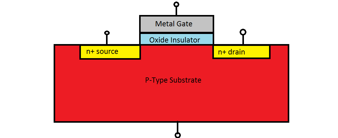
MOSFETS incorporate a MOS Capacitor that is next to two anti-doped regions. When no voltage is applied to the gate, the switch is off, and current cannot flow between the source and drain contacts. This is because free electrons from the source immediately recombine with holes once they reach the p-doped region. Put another way, when the switch is off, current cannot flow between the n-doped regions no matter the voltage applied because at one side there will be a pn junction in reverse bias.
When voltage is applied to the gate of the MOS capacitor, it creates an electric field which brings free electron charge carriers to the contact surface between the insulator and semiconductor. Initially this creates a depletion region, and then an inversion layer forms where free electrons dominate. This inversion layer is a conduction channel between the n-doped regions, which allows current to flow, and the switch is on. The gate voltage required for this effect is called the threshold voltage, because before this voltage no current can flow. This electric field effect on the semiconductor charge carriers is the MOSFET's namesake.
Pinch-Off Effect
The inversion layer in a MOSFET that is conducting is not symmetrical. An illustration of the inversion layer in this case is in Figure 2. In the inversion layer, the current density is highest near the drain and lower near the source due to the asymmetrical shape.
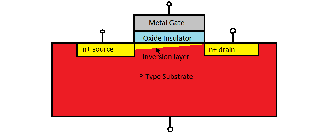
The slanted shape of the inversion layer is due to the fact that charge carriers along the channel experience a combination of voltage potentials from the gate, source, and drain. At the drain, there is higher voltage than at the source, so the electrons immediately under the gate next to the drain experience less influence from the gate; they are partially shielded. If the voltage difference between the source and drain is high enough, the inversion layer will pinch off before the drain, even in the presence of a greater-than-threshold gate voltage. This is the saturation voltage, and it is a limiting factor in the current a MOSFET can carry.
Fabrication
An illustration of MOSFET fabrication process is presented in figure 2.
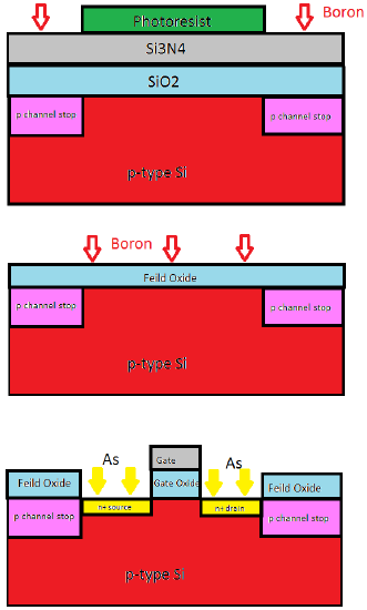
In making a MOSFET, first a lightly doped p-type Silicon wafer is used. \(SiO_2\) is grown over this and \(Si_3N_4\) is then deposited over that. The device region is protected by a layer of photo-resist, and then the surface is heavily doped with boron through the \(Si_3N_4\) and \(SiO_2\) into the wafer surface. This creates heavily doped p channel stop which prevent conduction between devices. Next, the SiO2 is etched away and a layer of field oxide is deposited, and more boron is doped in. This is to modify the doping concentration in the channel. Next, the field oxide is removed over the active device area and the gate oxide is grown in the center. A poly silicon layer is deposited on top of the gate and heavily doped to be conductive. Finally, arsenic atoms are doped to form the n+ drain and source regions. The gate itself shields the doping so that the regions are defined by the gate. This minimizes over-lap capacitance between the n+ regions and the gate.
Questions
- Q1: Why is the insulator present? What would happen to the device if it were absent?
- Q2: If the gate voltage is nonzero but below the threshold voltage, and the source to drain voltage is zero, what does the inversion layer look like?
- Q3: How does the device fail if it gets too hot? Will it be pinned open or closed?
--------------------------------------------------
- A1:If the metal gate made direct contact to the semiconductor, when voltage was applied it would conduct current directly from the source, and the device would not operate properly.
- A2:The inversion layer will not be present. There will be a depletion region at the oxide contact surface, but because it is below the threshold voltage, not enough carriers are drawn to the surface to create an inversion layer. The depletion layer will be flat along the length of the device because there is no horizontal voltage gradient to slant it.
- A3: THe device will be pinned open. When the MOSFET is too hot, thermally excited carriers will dominate and the depletion zone between the source and drain will dissipate, allowing current flow.
References
- Neaman, Donald. An Introduction to Semiconductor Devices. McGraw-Hill, 2006. 223-335. Print.
- S.O Kasap, Principles of electronic Materials and Devices, 3rd ed. McGraw-Hill, 2005, ISBN 0073104647
- Harris, Randy, and Randy Harris. Modern Physics. Second ed. San Francisco: Pearson/Addison Wesley, 2008. 212. Print.