
4.2: 3-Address CPU
- Page ID
- 76110

At the most basic level, there are 3 main components to a CPU: the ALU, memory (registers), and a Control Unit (CU). This is illustrated in the following figure showing a very basic and generic 3-Address CPU with 8 registers.
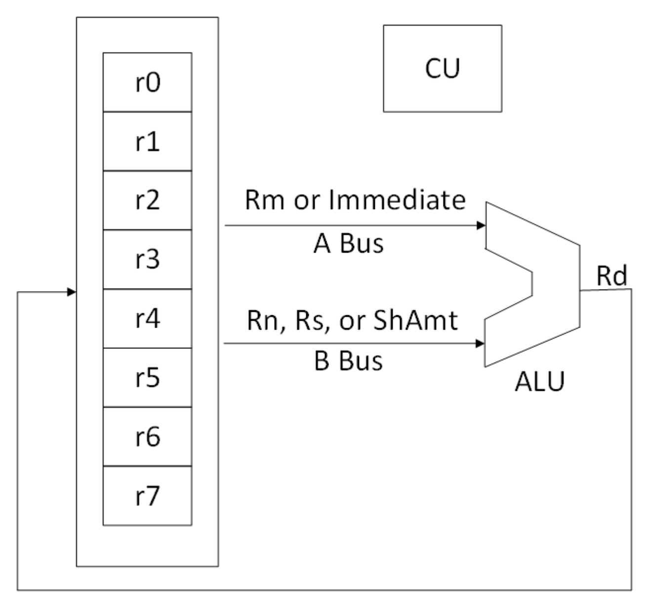
Figure 11: 3-Address CPU
There are a number of details that need to be covered regarding this diagram. First, there are 16 registers accessible in user mode in the ARM architecture. The first 12 will be usable in this chapter, though the first 4 (0-3) are somewhat different from the next 8 (4-12). This difference will be covered in Chapter 7 on functions. The final 3 registers are used for special purposes in ARM and have special names. The register r13 is called the stack pointer (sp), register r14 is called the link register (lr), and register r15 is called the pc. These registers are special in the ARM CPU and should only be used for their intended purposed. These registers will be covered in chapter 7.
Next, the lines with arrow in the diagram are actually 32 wires, each carrying one bit, and together called a bus. The top set of wires from Register Bank to the ALU is named the A Bus, and the bottom wire from the Register Bank to the ALU is named the B Bus.
From the point of view of the assembly programmer, there are two basic formats for the instructions. The first format uses one destination register and two source registers.
OP \(\rm R_d\), \(\rm R_1\), \(\rm R_2\) // meaning is \(\rm R_d\) ← \(\rm R_1\) OP \(\rm R_2\) where OP is the operator
The second format uses one destination register, but the source is one register and a numeric value.
OP \(\rm R_d\), \(\rm R_1\), #num // meaning is \(\rm R_d\) ← \(\rm R_1\) OP #num where OP is the operator
If this was a book about 3-Address assembly, this would be enough of a definition of the instructions. When writing assembly language for the problems at the end of this chapter, it is complete enough. However, this book is about ARM assembly, and so the correct registers and numeric values must follow the ARM conventions. These conventions will make more sense after covering chapter 5, but for now there are many comments online by ARM assembly programmers about how the register conventions for the instructions seem almost random. For this chapter, these conventions will almost seem random.
The data on the A Bus can either be a value from a register in the register bank, or an immediate value. An immediate value is a number that is specified as part of the assembly instruction.
Note that for this 3-address CPU, an immediate value is always an 8-bit signed integer from -128 ... 127. In the following example, the immediate value 87 is used on the A Bus.
ADD r1, r2, #87
If the A Bus gets its value from a register, then register identifier Rm will be used to specify the register number. In the following example the value in r4 is used on the A Bus, so Rm would be the 4-bit register identifier 0b0100. Remember the value placed on the bus is the 32-bit value in register r4, not the register number. For example, in the following add instruction where Rm is r4 and register r4 contains the value 87, the value passed to the ALU is 87.
ADD r1, r2, r4
The data on the B Bus is again either a value from a register, or a number called a Shift Amount (ShAmt). The ShAmt is a 5-bit number from 0 ... 31 and again is included in the instruction. For example, the following command shifts r1 2 bytes to the left.
LSL r1, r1, #2
If the value on the B Bus is a register, it can either be the Rn or Rs register. Most instructions will use Rn, but some like multiply or shift, will use Rs. The reason for this will be covered in Chapter 5. However, to properly document the instructions in this chapter realize that Rn and Rs both represent registers whose values are sent on the B Bus. In the following example the Rd register is r1, Rn is r2, and Rm is r3.
ADD r1, r2, r3
For this chapter, just think of assembly using \(R_1, R_2\), and #num as operands, though the documentation of the operators at the end of the chapter will use the real names to be consistent with the rest of the text and real ARM assembly. And while it might seem like all of this is just useless information, it does matter, and Chapter 6 cannot be understood without it.
The next part of the CPU to look at is the CU. The purpose of the CU is to translate the assembly language into control wires used by the CPU to specify how the CPU executes a given instruction. It is beyond the scope of this textbook and so will not be covered any further in this textbook and will not appear on any future diagrams.
The last detail to cover is the most important. The main purpose of a CPU is do calculations, and those calculations are done in the calculation unit, generally the ALU. Other than branching logic (which will not be covered in this chapter), the purpose of the CPU can be seen as getting the correct data from memory into registers, sending the values of registers to the ALU for execution, and storing the results back to a register, and storing register values back to memory.
There are two types of instructions that are available for this 3-address CPU. The first type of instruction uses two registers values as input to the ALU, with the ALU producing a result value that is saved to a register. This type of instruction looks as follows:
ADD r1, r2, r3
This statement says to add r2 and r3, storing the value in r1, or r1 ← r2 + r3.
The second type of instruction specifies one input register and one immediate value to a register and the register to save the value to. This type of instruction looks as follows:
ADD r1, r2, #3
This statement says to add r2 and #3, storing the value in r1, or r1 ← r2 + #3.
Note that in both cases, the add needs 3 operands (or addresses). In the first case the operands are three registers, and in the second case the operands are two registers and an immediate. But there are always 3 operands (or addresses) for every instruction, and this is why it is called a 3- address architecture.