
8.1: Carrier Dynamics and Saturation Properties
- Page ID
- 44669

There is a rich ultrafast carrier dynamics in these materials, which can be favorably exploited for saturable absorber design. The carrier dynamics in bulk semiconductors occurs on three major time scales (see Figure 8.4 [5]). When electron-hole pairs are generated, this excitation can be considered as an equivalent two-level system if the interaction between the carriers is neglected, which is a very rough assumption.
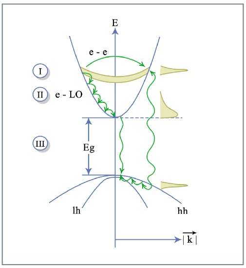
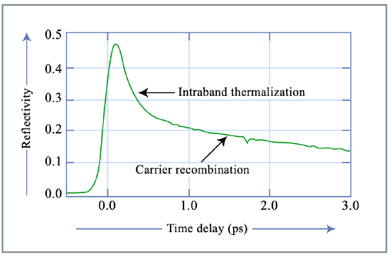
There is a coherent regime (I) with a duration of 10-50 fs depending on conditions and material. Then in phase (II), carrier-carrier scattering sets in and leads to destruction of coherence and thermalization of the electron and hole gas at a high temperature due to the excitation of the carriers high in the conduction or valence band. This usually happens on a 60 - 100 fs time scale. On a 300fs - 1ps time scale, the hot carrier gas interacts with the lattice mainly by emitting LO-phonons (37 meV in GaAs). The carrier gas cools down to lattice temperature. After the thermalization and cooling processes, the carriers are at the bottom of the conduction and valence band,respectively. The carriers vanish (III) either by getting trapped in impurity states, which can happen on a 100 fs - 100 ps time scale, or recombine over recombination centers or by radiation on a nanosecond time-scale. Carrier-lifetimes in III-VI semiconductors can reach several tens of nanoseconds and in indirect semiconductors like silicon or germanium lifetimes can be in the millisecond range. The carrier lifetime can be engineered over a large range of values from 100 fs - 30ns, depending on the growth conditions and purity of the material. Special low-temperature growth that leads to the formation or trapping and recombination centers as well as ion-bombardment can result in very short lifetimes [9]. Figure 8.5 shows a typical pump probe response of a semiconductor saturable absorber when excited with a 100 fs long pulse. The typical bi-temporal behavior stems from the fast thermalization (spectral hole-burning)[7] and carrier cooling and the slow trapping and recombination processes.
With the formula for the saturation intensity of a two-level system Equation (2.4.7), we can estimate a typical value for the saturation fluence \(F_s\) (saturation energy density) of a semiconductor absorber for interband transitions. The saturation fluence \(F_A\), also related to the absorption cross-section \(\sigma_A\), is then given by
\[F_A = \dfrac{hf}{\sigma_A} = I_A \tau_A = \dfrac{\hbar^2}{2T_2Z_F |\bar{M}|^2} \nonumber \]
\[= \dfrac{\hbar^2 n_0}{2T_2 Z_{F0} |\bar{M}|^2} \nonumber \]
The value for the dipole moment for interband transitions in III-V semicon-ductors is about \(d = 0.5\) nm with little variation for the different materials. Together with the a dephasing time on the order of \(T_2 = 20\) fs and a linear refractive index \(n_0 = 3\), we obtain
\[F_A = \dfrac{\hbar^2 n_0}{2T_2 Z_{F0} |\bar{M}|^2} = 35 \dfrac{\mu J}{cm^2} \nonumber \]
Figure 8.6 shows the saturation fluence measurement and pump probe trace with 10 fs excitation pulses at 800 nm on a broadband GaAs semiconductor saturable absorber based on a metal mirror shown in Figure 8.7 [11]. The pump probe trace shows a 50 fs thermalization time and long time bleaching of the absorption recovering on a 50 ps time scale due to trapping and recombination.
Image removed due to copyright restrictions. Please see: Jung, I. D., et al. "Semiconductor saturable absorber mirrors supporting sub-10 fs pulses." Applied Physics B 65 (1997): 137-150. Figure 8.6: Saturation fluence and pump probe measurements with 10 fs pulses on a broadband metal mirror based GaAs saturable absorber. The dots are measured values and the solid line is the fit to a two-level saturation characteristic [11].
A typical value for the fluence at which damage is observed on an absorber is on the order of a few \(\text{mJ}/\text{cm}^2\). Saturating an absorber by a factor of 10 without damaging it is still possible . The damage threshold is strongly dependent on the growth, design, fabrication and mounting (heat sinking) of the absorber.
Image removed due to copyright restrictions. Please see: Fluck, R., et al. "Broadband saturable absorber for 10 fs pulse generation." Optics Letters 21 (1996): 743-745. Figure 8.7: GaAs saturable absorber grown an GaAs wafer and transfered onto a metal mirror by post growth processing [10].