
3.12: Electrostatic Discharge and Latch-Up
- Page ID
- 88544

As you are probably aware, you have to be very careful when handling MOS circuits to be sure that you are properly grounded, and that you do not transfer any static electricity to the chip. The standard human-body model assumes a static charge transfer of about 0.1 micro-Coulombs \(10^{-7} \mathrm{C}\) upon static electricity discharge between a human and a chip. This does not seem like enough charge to do any harm until we remember the old formula: \[Q = CV\] or \[V = \frac{Q}{C}\]
Last time I looked, \(10^{-7}\) divided by \(10^{-14}\) is about \(10^{7}\) volts! Add to this the fact that the gate oxide thickness is only about \(10^{-6} \mathrm{~cm}\), so that we have electric fields in the gate oxide which are on the order of \(10^{13} \ \frac{\mathrm{V}}{\mathrm{cm}}\)! No wonder the things break. This problem is called electrostatic discharge, or ESD, and is one of the major concerns of IC manufacturers. Protecting against ESD is still very much a "black art" and is something that people are still studying quite a bit. JFETs are much more rugged structures with have much higher gate capacitances, and are not nearly so prone to ESD failure.
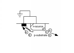
Since we are on the subject of problems, lets take a look at one more "glitch" that plagues IC designers. We have to go back to the CMOS circuit. Remember, the moat/substrate junction is reverse biased, so we will have an electric field in the depletion region of that junction, pointing as shown in Figure \(\PageIndex{1}\).
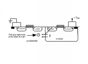
Suppose, somehow, we have one or more stray electrons in the p-type substrate. They will be swept across the substrate/moat junction by the electric field, and be attracted to the moat contact by \(V_{\text{dd}}\). Let's focus on what happens as the electron flows out the \(V_{\text{dd}}\) contact (Figure \(\PageIndex{2}\)).
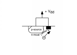
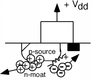
As the electron moves through the (resistive) n-type moat material, it develops a voltage drop between the n-type material under the source, and the \(V_{\text{dd}}\) contact (which is also at the source potential since they are connected together by the interconnect on the surface of the wafer). Electron flow in one direction means current flow in the other, and so this makes the region under the source slightly negative with respect to the source region itself. This, of course, forward biases the source/moat junction slightly, which causes a hole or two to be injected into the moat from the p-source (Figure \(\PageIndex{3}\)).
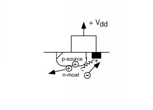 Figure \(\PageIndex{3}\): The forward biased source injects some holes
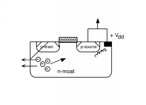
The holes will be attracted by the field across the moat-substrate depletion layer, and, once they get there, they will be swept into the p-substrate (Figure \(\PageIndex{4}\)).
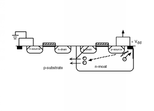
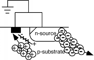
Once the holes get into the p-substrate, they will be attracted to the ground connection so that they can leave the semiconductor. As these holes flow past the n-source, and through the resistive p-substrate, they build up a potential between the ground contact (Figure \(\PageIndex{5}\)), and the material under the source with a polarity which tends to forward bias the source-substrate junction, and cause electrons to be injected into the substrate. The electrons, in turn, are attracted to the field across the substrate-moat junction (Figure \(\PageIndex{6}\)).
Some of the electrons may recombine in the p-region, but in today's high-quality substrates, there are very few active recombination centers, and so even though the electrons are minority carriers, they have quite a long minority carrier lifetime, and most of them make it to the substrate-moat junction and are swept into the moat. Once inside the n-moat, the electrons are then attracted to the \(+V_{\text{dd}}\) contact, where, of course, they build up a bigger forward bias across the source-moat junction, causing more holes to be emitted from the source into the moat (Figure \(\PageIndex{7}\)). These holes are swept across the moat-substrate junction, flow to the ground contact and, well ... you get the idea! It does not take long before we have a dead short circuit between Vdd and ground. This is not healthy for integrated circuit chips in the least, and is a process called latch-up (Figure \(\PageIndex{8}\)).
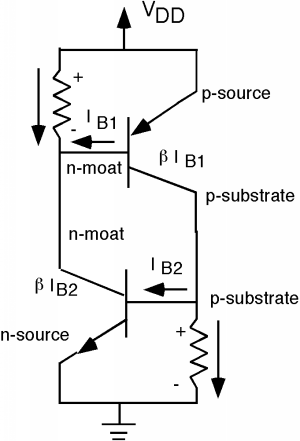
There is an interesting circuit you can draw which shows what is happening from a somewhat different point of view. Note that we can consider the p-source, n-moat, and p-substrate as a pnp bipolar transistor. Also the n-source, p-substrate and n-moat also make a fine npn bipolar transistor. The two transistors are intermingled however, with the base of the pnp and the collectors of the npn sharing the same n-moat, and the collector of the pnp and the base of the npn sharing the p-substrate. The n-moat and p-substrates are both collectors and bases at the same time. A little careful inspection of the cross section of the CMOS inverter will lead you to the following schematic shown in Figure \(\PageIndex{9}\). We need something to get this circuit started, so say we have a little collector current coming out of the top pnp transistor. This current flows down, through the resistor to ground. As it flows through the resistor it builds up a little voltage which forward biases the base-emitter junction of the lower, npn, transistor, and causes some collector current to flow into it. This current comes from \(V_{\text{dd}}\) through the upper resistor, and builds up a voltage across that resistor which will forward bias the base-emitter junction of the top, pnp, transistor. This, in turn, causes some additional collector current to flow out of the pnp transistor, and away we go! Latch-up is bad, and is something which IC designers work very hard to avoid.
You might wonder what actually starts a circuit going into latch-up. Refer back to the CMOS inverter, and note that the n-drain on the NMOS is connected to the output. The output could be a real output, going beyond the chip into the "real world". If the "customer" who is using the chip is careless, and somehow drags the output down below ground, the drain/p-substrate junction will be forward biased, electrons will be injected into the p-substrate, and we are back at Figure \(\PageIndex{1}\). IC designers try to keep the n-moat/\(V_{\text{dd}}\) contact as close to the PMOS source, and the p-substrate/ground contact as close to the NMOS source as they can to reduce the resistance between the contact and the source regions, and hence lower the chance of the circuit going into latch-up.