
5.4: Switch


( \newcommand{\kernel}{\mathrm{null}\,}\)
Microwave switches are commonly used to alternately connect an antenna to a transmitter or a receiver. In some communication systems, such as GSM and some modes of 4G and 5G, a phone does not transmit and receive simultaneously. Consequently a switch can be used to separate the transmitted and received signals. In multiband phones, a switch is used to connect the correct transmitter and receiver, which are band specific, to the antenna. In radar systems, switches are used to steer an antenna beam by changing the phase of the microwave signal delivered to each antenna in an array of antennas. An ideal microwave switch is shown in Figure 5.4.1(a), where an input port, RFIN, and an output port, RFOUT, are shown. For maximum power transfer between the ports the switch should have little loss and thus have low on resistance. At microwave frequencies, realistic switches must be modeled with parasitics and with finite on and off resistances. A realistic model applicable to many switch types is shown in Figure 5.4.1(b). The capacitive parasitics, the CPs, limit the frequency of operation of the switches and the on resistance, RON, impacts the switch loss. Ideally the off resistance, ROFF, is very large, however, the parasitic shunt capacitance, COFF, is nearly always more significant. The result is that at high frequencies there is an alternative capacitive connection between the input and output through COFF. The on resistance of the switch introduces voltage division that can be seen by comparing the ideal connection shown in Figure 5.4.1(c) and the more realistic connection shown in Figure 5.4.1(d). From the voltage division ratio, the loss of the switch can be calculated.
Switches are configured to provide connections from one or more inputs to one or more outputs. The configuration of a switch is indicated by poles and throws, and several configurations are shown in Figure 5.4.2. In microwave applications, single-pole switches are most commonly used and the input is connected to an antenna. For example, the throws would be connected to different bands of a multiband phone.
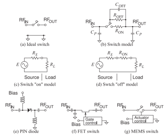
Figure 5.4.1: Microwave switches: (a) ideal switch connecting RFIN and RFOUT ports; (b) model of a microwave switch; (c) ideal circuit model with switch on and with source and load; (d) realistic low-frequency circuit model with the switch on; (e) switch realized using a PIN diode; (f) switch realized using an FET; and (g) switch realized using a MEMS switch.
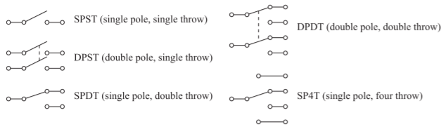
Figure 5.4.2: Switch configurations.
| Switch type | Configuration | Power handling | Maximum insertion loss | Operating frequency | Actuation voltage | Response time |
|---|---|---|---|---|---|---|
| MEMS1 | SPDT | 0.5 W | 0.5 dB | to 10 GHz | 90 V | 10μs |
| MEMS1 | SPDT | 4 W | 0.8 dB | to 35 GHz | 110 V | 10μs |
| FET (pHEMT)2 | SPDT | 10 W | 0.3 dB | to 6.5 GHz | 5 V | 0.5μs |
| FET (pHEMT)2 | SPDT | 0.3 W | 1.1 dB | to 25 GHz | 5 V | 0.5μs |
| PIN3 | SPDT | 13 W | 0.35 dB | to 2 GHz | 12 V | 0.5μs |
| PIN3 | SPDT | 10 W | 0.4 dB | to 6 GHz | 12 V | 0.5μs |
| FET (SOI)4 | SPDT | 2 W | 2.7 dB | to 60 GHz | 3.6 V | 8 ns |
Table 5.4.1: Typical properties of small microwave switches. (Sources: 1Radant MEMS, 2RF Micro Devices, 3Tyco Electronics,and 2pSemiTM Corporation.)
There are four main types of microwave switches: mechanical, PIN diode, FET, and microelectromechanical system (MEMS) switches. Mechanical switches are nearly lossless but tend to be large, relatively expensive, slow to operate, and are mostly used in laboratory settings. The other switches are of most interest for use in systems. The PIN diode, FET, and MEMS switches are shown in Figures 5.4.1(e–g), respectively. With these technologies, most higher-order switches are based on interconnections of SPST switches. The attributes of these switches are summarized in Table 5.4.1 for switches that are suitable for cell phone applications. PIN diode switches are the most robust, handling the most RF power, and operating at higher frequencies than either FET- or MEMS-based switches. However, this comes at a price. The PIN diode used is similar to a pn junction diode with the addition of an intrinsic layer between the p- and n-type materials. With applied forward bias the diode has low RF series resistance. In reverse bias, the diode RF resistance is large. Forward bias requires DC current and voltage, so control power is consumed when a PIN diode switch is on. The circuit configuration for an SPST PIN diode switch is shown in Figure 5.4.1(e). Series bias-decoupling capacitors are required at the RF ports.
A FET makes a good electronic switch; with the correct bias applied to the gate, the drain-source connection looks like a small resistance. Changing the bias to the other extreme removes free carriers from the channel between the drain and source, and a large resistance is the result. Both Si and GaAs
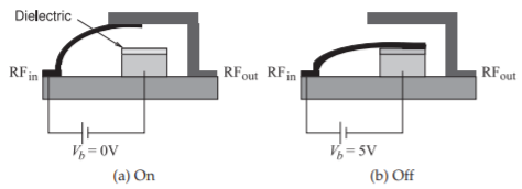
Figure 5.4.3: RF MEMS switch: (a) the RFin line in contact with the RFout line; and (b) the cantlever beam electrostatically attracted to the pedestal and there is no RF connection.
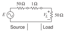
Figure 5.4.4: Model used in calculating the loss of a switch in a 50Ω system.
switches are used in cellular handsets, with GaAs switches operating at extended frequencies approaching 6 GHz. The operation of a FET can be described as a variable drain-source resistance with the gate-source voltage controlling the cross section of the channel. The circuit for a FET-based SPST switch is shown in Figure 5.4.1(f). Series bias-blocking capacitors are required at the RF ports. Control power is only required to change the state of the switch; negligible power is required to maintain the switch state.
A MEMS switch is fabricated using photolithographic techniques similar to those used in semiconductor manufacturing [11, 12, 13]. They are essentially miniature mechanical switches with a voltage used to control the position of a shorting arm, which is usually a cantilever or a membrane, see Figure 5.4.3. As there is no direct connection between the RF signal path and the control circuitry, MEMS switches have inherently high operating frequencies. Power is required to change the switch, but once switching has been accomplished, negligible DC power is required to maintain the connection. Two of the major problems are creating the contact with enough force to reduce the series resistance, and maintaining the structural integrity of the contacts after hundreds of millions of cycles. Generally it is not necessary to make a DC contact, and creating a structure that has a large difference between the on capacitance and off capacitance is sufficient for applications such as tunable matching networks [11].
Example 5.4.1: Insertion Loss of a Switch
What is the insertion loss of a switch with a 1Ω on resistance when it used in a 50Ω system?
Solution
The model to be used for evaluating the insertion loss of the switch is shown in Figure 5.4.4. The insertion loss is found by first determining the available power from the source and then the actual power delivered to the load. The available input power is calculated by first ignoring the 1Ω switch resistance. Then there is maximum power transfer from the source to the load. The available input power is
PAi=12(12E)250=E2400
where E is the peak RF voltage at the Thevenin equivalent source generator. The power delivered to the 50Ω load is found after first determining the peak load voltage:
VL=5050+1+50E=50101E
Thus the power delivered to the load is
PD=12V2L50=1100(50101)2E2
The insertion loss is
IL=PAiPD=E2400100E2(10150)2=1.020=0.086 dB