
Metal-Oxide-Semiconductor (MOS) Fundamentals
- Page ID
- 366
\( \newcommand{\vecs}[1]{\overset { \scriptstyle \rightharpoonup} {\mathbf{#1}} } \)
\( \newcommand{\vecd}[1]{\overset{-\!-\!\rightharpoonup}{\vphantom{a}\smash {#1}}} \)
\( \newcommand{\dsum}{\displaystyle\sum\limits} \)
\( \newcommand{\dint}{\displaystyle\int\limits} \)
\( \newcommand{\dlim}{\displaystyle\lim\limits} \)
\( \newcommand{\id}{\mathrm{id}}\) \( \newcommand{\Span}{\mathrm{span}}\)
( \newcommand{\kernel}{\mathrm{null}\,}\) \( \newcommand{\range}{\mathrm{range}\,}\)
\( \newcommand{\RealPart}{\mathrm{Re}}\) \( \newcommand{\ImaginaryPart}{\mathrm{Im}}\)
\( \newcommand{\Argument}{\mathrm{Arg}}\) \( \newcommand{\norm}[1]{\| #1 \|}\)
\( \newcommand{\inner}[2]{\langle #1, #2 \rangle}\)
\( \newcommand{\Span}{\mathrm{span}}\)
\( \newcommand{\id}{\mathrm{id}}\)
\( \newcommand{\Span}{\mathrm{span}}\)
\( \newcommand{\kernel}{\mathrm{null}\,}\)
\( \newcommand{\range}{\mathrm{range}\,}\)
\( \newcommand{\RealPart}{\mathrm{Re}}\)
\( \newcommand{\ImaginaryPart}{\mathrm{Im}}\)
\( \newcommand{\Argument}{\mathrm{Arg}}\)
\( \newcommand{\norm}[1]{\| #1 \|}\)
\( \newcommand{\inner}[2]{\langle #1, #2 \rangle}\)
\( \newcommand{\Span}{\mathrm{span}}\) \( \newcommand{\AA}{\unicode[.8,0]{x212B}}\)
\( \newcommand{\vectorA}[1]{\vec{#1}} % arrow\)
\( \newcommand{\vectorAt}[1]{\vec{\text{#1}}} % arrow\)
\( \newcommand{\vectorB}[1]{\overset { \scriptstyle \rightharpoonup} {\mathbf{#1}} } \)
\( \newcommand{\vectorC}[1]{\textbf{#1}} \)
\( \newcommand{\vectorD}[1]{\overrightarrow{#1}} \)
\( \newcommand{\vectorDt}[1]{\overrightarrow{\text{#1}}} \)
\( \newcommand{\vectE}[1]{\overset{-\!-\!\rightharpoonup}{\vphantom{a}\smash{\mathbf {#1}}}} \)
\( \newcommand{\vecs}[1]{\overset { \scriptstyle \rightharpoonup} {\mathbf{#1}} } \)
\(\newcommand{\longvect}{\overrightarrow}\)
\( \newcommand{\vecd}[1]{\overset{-\!-\!\rightharpoonup}{\vphantom{a}\smash {#1}}} \)
\(\newcommand{\avec}{\mathbf a}\) \(\newcommand{\bvec}{\mathbf b}\) \(\newcommand{\cvec}{\mathbf c}\) \(\newcommand{\dvec}{\mathbf d}\) \(\newcommand{\dtil}{\widetilde{\mathbf d}}\) \(\newcommand{\evec}{\mathbf e}\) \(\newcommand{\fvec}{\mathbf f}\) \(\newcommand{\nvec}{\mathbf n}\) \(\newcommand{\pvec}{\mathbf p}\) \(\newcommand{\qvec}{\mathbf q}\) \(\newcommand{\svec}{\mathbf s}\) \(\newcommand{\tvec}{\mathbf t}\) \(\newcommand{\uvec}{\mathbf u}\) \(\newcommand{\vvec}{\mathbf v}\) \(\newcommand{\wvec}{\mathbf w}\) \(\newcommand{\xvec}{\mathbf x}\) \(\newcommand{\yvec}{\mathbf y}\) \(\newcommand{\zvec}{\mathbf z}\) \(\newcommand{\rvec}{\mathbf r}\) \(\newcommand{\mvec}{\mathbf m}\) \(\newcommand{\zerovec}{\mathbf 0}\) \(\newcommand{\onevec}{\mathbf 1}\) \(\newcommand{\real}{\mathbb R}\) \(\newcommand{\twovec}[2]{\left[\begin{array}{r}#1 \\ #2 \end{array}\right]}\) \(\newcommand{\ctwovec}[2]{\left[\begin{array}{c}#1 \\ #2 \end{array}\right]}\) \(\newcommand{\threevec}[3]{\left[\begin{array}{r}#1 \\ #2 \\ #3 \end{array}\right]}\) \(\newcommand{\cthreevec}[3]{\left[\begin{array}{c}#1 \\ #2 \\ #3 \end{array}\right]}\) \(\newcommand{\fourvec}[4]{\left[\begin{array}{r}#1 \\ #2 \\ #3 \\ #4 \end{array}\right]}\) \(\newcommand{\cfourvec}[4]{\left[\begin{array}{c}#1 \\ #2 \\ #3 \\ #4 \end{array}\right]}\) \(\newcommand{\fivevec}[5]{\left[\begin{array}{r}#1 \\ #2 \\ #3 \\ #4 \\ #5 \\ \end{array}\right]}\) \(\newcommand{\cfivevec}[5]{\left[\begin{array}{c}#1 \\ #2 \\ #3 \\ #4 \\ #5 \\ \end{array}\right]}\) \(\newcommand{\mattwo}[4]{\left[\begin{array}{rr}#1 \amp #2 \\ #3 \amp #4 \\ \end{array}\right]}\) \(\newcommand{\laspan}[1]{\text{Span}\{#1\}}\) \(\newcommand{\bcal}{\cal B}\) \(\newcommand{\ccal}{\cal C}\) \(\newcommand{\scal}{\cal S}\) \(\newcommand{\wcal}{\cal W}\) \(\newcommand{\ecal}{\cal E}\) \(\newcommand{\coords}[2]{\left\{#1\right\}_{#2}}\) \(\newcommand{\gray}[1]{\color{gray}{#1}}\) \(\newcommand{\lgray}[1]{\color{lightgray}{#1}}\) \(\newcommand{\rank}{\operatorname{rank}}\) \(\newcommand{\row}{\text{Row}}\) \(\newcommand{\col}{\text{Col}}\) \(\renewcommand{\row}{\text{Row}}\) \(\newcommand{\nul}{\text{Nul}}\) \(\newcommand{\var}{\text{Var}}\) \(\newcommand{\corr}{\text{corr}}\) \(\newcommand{\len}[1]{\left|#1\right|}\) \(\newcommand{\bbar}{\overline{\bvec}}\) \(\newcommand{\bhat}{\widehat{\bvec}}\) \(\newcommand{\bperp}{\bvec^\perp}\) \(\newcommand{\xhat}{\widehat{\xvec}}\) \(\newcommand{\vhat}{\widehat{\vvec}}\) \(\newcommand{\uhat}{\widehat{\uvec}}\) \(\newcommand{\what}{\widehat{\wvec}}\) \(\newcommand{\Sighat}{\widehat{\Sigma}}\) \(\newcommand{\lt}{<}\) \(\newcommand{\gt}{>}\) \(\newcommand{\amp}{&}\) \(\definecolor{fillinmathshade}{gray}{0.9}\)The metal-oxide (SiO2)-semiconductor (Si) is the most common microelectronic structures nowadays. The two terminals of MOS-Capacitor consist of the main structures in MOS devices and it is the simplest structure of MOS devices. Therefore, it's essential to understand the mechanisms and characteristics of how MOS-C operates. The mechanisms under static biasing conditions can be visualized from two diagrams.
- Energy band diagram
- Block-charge diagram
The characteristics of MOS-C can be visualized by C-V (Capacitance verses Voltage) curves.
Introduction
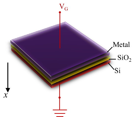
The principals of forming MOS structure are similar to the metal-semiconductor (MS) contact structures, but the MOS structure is like a sandwich structure which have a thin layer of silicon oxides in the middle between metal and semiconductor (Si) layer. Figure 1 below shows a schematic of an ideal MOS-C device. For an ideal MOS-C structure, some properties should follow below.
- The metallic gate should thick enough to be equipotential region, where every points has the same potential in the space, under a.c and d.c biasing conditions.
- The oxides layer in the middle should be a perfect insulator with zero current flowing through under all static biasing conditions.
- There should be no charge centers located on the oxide-semiconductor interface.
- The semiconductor should be uniformly doped with donors or acceptors as p-type or n-type semiconductors.
- The semiconductor (Si) should be thick enough for charges to encounter a field free region (Si bulk) before reaching the back contact.
- The Ohmic contacts should be established on the backside of the MOS device.
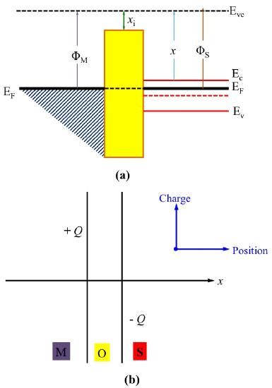
- MOS-C is a one-dimensional structure with variables only related to the x-coordinate (distance) as the Figure 1 below.
- The metal work function (Φ M) should equal to the semiconductor work function (Φ S) as well as the electron affinity (X) with the difference of conduction band (Ec) and Fermi energy (E F) in forward flat band, Φ M=Φ S=χ+(Ec−E F) FB. This property can be omitted, but it is easier to help with the initial understanding of the static behavior in MOS devices.
Energy Band and Block Charge Diagrams
The band diagram shows the band energy of the materials and how their energy levels change in the process as functions of spatial dimensions. The X-axis represents the distance (x) in the cross-section view of the MOS devices. The Y-axis represents the energy. There are no arbitrary values for Y but only relative values. As the Y-axis is increasing, the corresponding energy is higher. In the figure 2 below is the energy band diagram of MOS-C in flat band with n-type semiconductor. The E vc is the vacuum level which is th minimum energy an electron must reach in order to free from the material. The work function ΦM and ΦS are the amount of work to remove an electron, so it's the difference between Fermi level (E F) and E vc . The electron affinity (X) specifies the height of energy barrier in semiconductors, so the X i is the energy barrier of the insulator (oxides SiO 2). The zero-bias band diagram in figure 2 (a) is called flat band diagram. The formation of this band diagram can conceptually think of the equilibrium metal-semiconductor contact but is separated with a distance x0, the thickness of the oxide layer.The Fermi level aligned between metal and semiconductor since it's specified in the property 8 above. Since there are no charge or electric field in the flat band MOS-C device, the inserted insulator can only have an effect in slightly lowering the energy barrier and there is no block charge diagram for flat band like figure in 2(b).
The block charge diagram shows the charge density distribution inside the MOS structure. Like the energy band diagram, the X-axis represents the distance (x) in the cross-section view. However, the Y-axis represents the exact charge distribution Q in the MOS devices. There are two horizontal Y-axis which represent the metal-oxides interface and oxide-semiconductor interfaces. The region above X-axis is the positive charge Q which is created by holes concentration, while the region below X-axis is the negative charge Q which is created by electrons concentration.
Effect of an applied bias
Other than the flat band in the MOS structure, as the d.c bias VG apply to the MOS-C devices. Three different types of biasing regions with different shape of both energy band and corresponding block charge diagram occur and they are showed in figure 3, 4, 5 and 6 below for n-type semiconductors. However, the types of biasing regions are also different from n-type and p-type semiconductor because of the different positions of the Fermi level as well as the doped charges. Since the focus is the mechanisms under biasing conditions, the p-type diagrams follow the same concepts but are not discussed here. One thing worth mentioning is that the Fermi level of semiconductor does not change when V G is applied. Therefore, the V G can be calculated as the equation (1) shown below, where q is the electric charge.
\[E F(Metal)-E F(Semiconductor)=-q*V G (1)\]
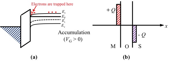
- The first type of biasing region is accumulation, where the majority carrier concentration is greater near the oxide-semiconductor interface than in the bulk of the semiconductor. This happens for n-type semiconductor when V G >0. From the band diagram view, the applied bias lowers the Fermi level of the metal below the Fermi level of the semiconductor. The Ec and Ev of the semiconductor also bend down following the principals of MS contact. The majority carriers for n-type semiconductors electrons are trapped on the interface between oxides-semiconductor shown on figure 3 (a). From the block charge diagram view, there are some positive charges accumulates on the metal gate because of the positive bias, the negatively excess electrons in the semiconductors are attracted toward the oxide-semiconductor interfaces shown in figure 3(b).
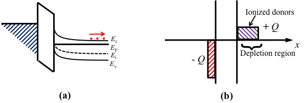
- The second type of biasing region is depletion, where the concentration of the majority carriers has been depleted. This happens for n-type semiconductor when VG<0 (small). From the band diagram view, the applied bias raises the Fermi level of the metal higher than the Fermi level of the semiconductor. The negative slope bending (up direction bending) occurs for the semiconductor. The donors (electrons) are moving to the opposite direction which is moving to the right in figure 4 (a). The concentrations of the donors have been decreasing, and this is so-called depletion. From the block charge diagram view, the applied negative bias repels the electrons on the semiconductors away from the MOS interfaces. Therefore, the electrons are on the surface of the semiconductor, so in figure 4 (b) the widths of block charge are wider than figure 3 (b). Also, in this case, the electron concentrations of the semiconductor are less than the background doping concentration ND.
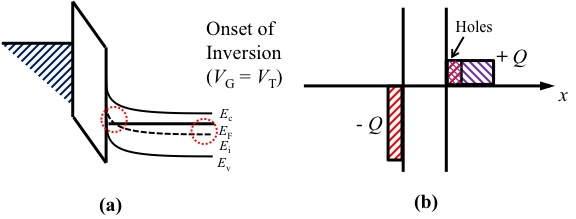
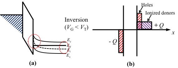
- The third type of biasing region inversion happens if the biasing voltages keep increasing from the depletion region. For example, for n-type semiconductor, if the V G<0 (big) is applying. The inversion biasing region is where the Fermi level of the semiconductor start cross out from above the Ei to below the Ei. The fact is emphasized by the red bubble in figure 5 (a). In the band diagram, the energy bands of semiconductor are bending more and more higher. The holes concentration at the surface increase as the concentration of the electrons decrease. At a threshold voltage (V T), the surface region changes from n-type to p-type as E F of the semiconductor cross the Ei. Therefore, the figure 5 represents the band diagram and block charge diagram for inversion biasing when the applied bias equals to the threshold voltage, V G=V T. The figure 6 represents the both diagrams for inversion biasing when the applied bias is larger than the threshold voltage, V G>V T. In the block charge diagram, since the applied bias is large enough the holes attracted to the interface piled up in figure 6 (b), and the ionized holes are on the surface as in figure 5 (b) and figure 6 (b).
C-V Characteristic Curve
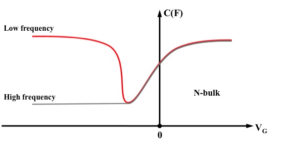
The capacitance of the MOS-C devices behave as the function of applied voltage V G. There are two limits: low frequency limit and high frequency limit. The behavior of both limits are shown in the Figure 7 for MOS-C device with n-type semiconductors. Their behaviors differ at inversion and inversion to transition regions but they converge at depletion, flat band and accumulation regions.
Conclusion
In summary, different types of biasing region depend on the biasing voltage applying to the MOS-C devices. Also, different doping of the n-type semiconductor and p-type semiconductor affects the biasing regions. The table 1 below shows the situation of how the MOS-C devices would be when specific VG is applying.
| Type / Applied Bias | VG=0 | V T>VG>0 (small) | VG>V T (Big) | V T<VG<0 (small) | VG<V T (Big) |
|---|---|---|---|---|---|
| n-type Semiconductor | Flat Band | VG>0 (small)" style="text-align:center;" class="lt-eng-366">Accumulation | V T (Big)" style="text-align:center;" class="lt-eng-366">Accumulation | Depletion | Inversion |
| p-type Semiconductor | Flat Band | VG>0 (small)" style="text-align:center;" class="lt-eng-366">Depletion | V T (Big)" style="text-align:center;" class="lt-eng-366">Inversion | Accumulation | Accumulation |
Questions
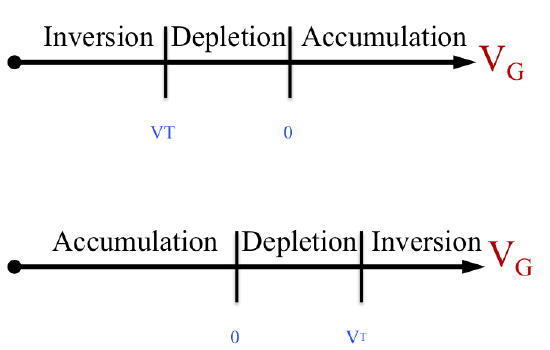
(1) Use a line plot to show the magnitude of V G ranges corresponding to accumulation, depletion, and inversion in ideal n-type and p-type MOS devices. Please include the marking of V T.
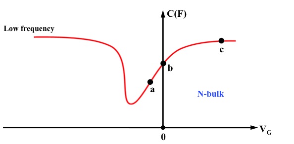
(2) What is the biasing region of the point a in the figure 8 below?
(3) What is the biasing region of the point b in the figure 8 below?
(4) What is the biasing region of the point c in the figure 8 below?
Answers
(1)
(2) Depletion
(3) Flat band
(4) Accumulation
References
- 1. Robert F. Pierret, Semiconductor Device Fundamentals, Second Edition. Chapter 16, pages 563-599.
- 2. Microelectronic Circuit Design, Jaeger, Blalock, Chapter 4, IEEE Standard MOS transistor circuit symbols.
- 3.B. Van Zeghbroeck, Principal of Electronic devices, 2011.
Contributors
- Xuan Mo (University of California, Davis, Materials Science and Engineering)