
Bipolar Junction Transistor
- Page ID
- 348
\( \newcommand{\vecs}[1]{\overset { \scriptstyle \rightharpoonup} {\mathbf{#1}} } \)
\( \newcommand{\vecd}[1]{\overset{-\!-\!\rightharpoonup}{\vphantom{a}\smash {#1}}} \)
\( \newcommand{\dsum}{\displaystyle\sum\limits} \)
\( \newcommand{\dint}{\displaystyle\int\limits} \)
\( \newcommand{\dlim}{\displaystyle\lim\limits} \)
\( \newcommand{\id}{\mathrm{id}}\) \( \newcommand{\Span}{\mathrm{span}}\)
( \newcommand{\kernel}{\mathrm{null}\,}\) \( \newcommand{\range}{\mathrm{range}\,}\)
\( \newcommand{\RealPart}{\mathrm{Re}}\) \( \newcommand{\ImaginaryPart}{\mathrm{Im}}\)
\( \newcommand{\Argument}{\mathrm{Arg}}\) \( \newcommand{\norm}[1]{\| #1 \|}\)
\( \newcommand{\inner}[2]{\langle #1, #2 \rangle}\)
\( \newcommand{\Span}{\mathrm{span}}\)
\( \newcommand{\id}{\mathrm{id}}\)
\( \newcommand{\Span}{\mathrm{span}}\)
\( \newcommand{\kernel}{\mathrm{null}\,}\)
\( \newcommand{\range}{\mathrm{range}\,}\)
\( \newcommand{\RealPart}{\mathrm{Re}}\)
\( \newcommand{\ImaginaryPart}{\mathrm{Im}}\)
\( \newcommand{\Argument}{\mathrm{Arg}}\)
\( \newcommand{\norm}[1]{\| #1 \|}\)
\( \newcommand{\inner}[2]{\langle #1, #2 \rangle}\)
\( \newcommand{\Span}{\mathrm{span}}\) \( \newcommand{\AA}{\unicode[.8,0]{x212B}}\)
\( \newcommand{\vectorA}[1]{\vec{#1}} % arrow\)
\( \newcommand{\vectorAt}[1]{\vec{\text{#1}}} % arrow\)
\( \newcommand{\vectorB}[1]{\overset { \scriptstyle \rightharpoonup} {\mathbf{#1}} } \)
\( \newcommand{\vectorC}[1]{\textbf{#1}} \)
\( \newcommand{\vectorD}[1]{\overrightarrow{#1}} \)
\( \newcommand{\vectorDt}[1]{\overrightarrow{\text{#1}}} \)
\( \newcommand{\vectE}[1]{\overset{-\!-\!\rightharpoonup}{\vphantom{a}\smash{\mathbf {#1}}}} \)
\( \newcommand{\vecs}[1]{\overset { \scriptstyle \rightharpoonup} {\mathbf{#1}} } \)
\(\newcommand{\longvect}{\overrightarrow}\)
\( \newcommand{\vecd}[1]{\overset{-\!-\!\rightharpoonup}{\vphantom{a}\smash {#1}}} \)
\(\newcommand{\avec}{\mathbf a}\) \(\newcommand{\bvec}{\mathbf b}\) \(\newcommand{\cvec}{\mathbf c}\) \(\newcommand{\dvec}{\mathbf d}\) \(\newcommand{\dtil}{\widetilde{\mathbf d}}\) \(\newcommand{\evec}{\mathbf e}\) \(\newcommand{\fvec}{\mathbf f}\) \(\newcommand{\nvec}{\mathbf n}\) \(\newcommand{\pvec}{\mathbf p}\) \(\newcommand{\qvec}{\mathbf q}\) \(\newcommand{\svec}{\mathbf s}\) \(\newcommand{\tvec}{\mathbf t}\) \(\newcommand{\uvec}{\mathbf u}\) \(\newcommand{\vvec}{\mathbf v}\) \(\newcommand{\wvec}{\mathbf w}\) \(\newcommand{\xvec}{\mathbf x}\) \(\newcommand{\yvec}{\mathbf y}\) \(\newcommand{\zvec}{\mathbf z}\) \(\newcommand{\rvec}{\mathbf r}\) \(\newcommand{\mvec}{\mathbf m}\) \(\newcommand{\zerovec}{\mathbf 0}\) \(\newcommand{\onevec}{\mathbf 1}\) \(\newcommand{\real}{\mathbb R}\) \(\newcommand{\twovec}[2]{\left[\begin{array}{r}#1 \\ #2 \end{array}\right]}\) \(\newcommand{\ctwovec}[2]{\left[\begin{array}{c}#1 \\ #2 \end{array}\right]}\) \(\newcommand{\threevec}[3]{\left[\begin{array}{r}#1 \\ #2 \\ #3 \end{array}\right]}\) \(\newcommand{\cthreevec}[3]{\left[\begin{array}{c}#1 \\ #2 \\ #3 \end{array}\right]}\) \(\newcommand{\fourvec}[4]{\left[\begin{array}{r}#1 \\ #2 \\ #3 \\ #4 \end{array}\right]}\) \(\newcommand{\cfourvec}[4]{\left[\begin{array}{c}#1 \\ #2 \\ #3 \\ #4 \end{array}\right]}\) \(\newcommand{\fivevec}[5]{\left[\begin{array}{r}#1 \\ #2 \\ #3 \\ #4 \\ #5 \\ \end{array}\right]}\) \(\newcommand{\cfivevec}[5]{\left[\begin{array}{c}#1 \\ #2 \\ #3 \\ #4 \\ #5 \\ \end{array}\right]}\) \(\newcommand{\mattwo}[4]{\left[\begin{array}{rr}#1 \amp #2 \\ #3 \amp #4 \\ \end{array}\right]}\) \(\newcommand{\laspan}[1]{\text{Span}\{#1\}}\) \(\newcommand{\bcal}{\cal B}\) \(\newcommand{\ccal}{\cal C}\) \(\newcommand{\scal}{\cal S}\) \(\newcommand{\wcal}{\cal W}\) \(\newcommand{\ecal}{\cal E}\) \(\newcommand{\coords}[2]{\left\{#1\right\}_{#2}}\) \(\newcommand{\gray}[1]{\color{gray}{#1}}\) \(\newcommand{\lgray}[1]{\color{lightgray}{#1}}\) \(\newcommand{\rank}{\operatorname{rank}}\) \(\newcommand{\row}{\text{Row}}\) \(\newcommand{\col}{\text{Col}}\) \(\renewcommand{\row}{\text{Row}}\) \(\newcommand{\nul}{\text{Nul}}\) \(\newcommand{\var}{\text{Var}}\) \(\newcommand{\corr}{\text{corr}}\) \(\newcommand{\len}[1]{\left|#1\right|}\) \(\newcommand{\bbar}{\overline{\bvec}}\) \(\newcommand{\bhat}{\widehat{\bvec}}\) \(\newcommand{\bperp}{\bvec^\perp}\) \(\newcommand{\xhat}{\widehat{\xvec}}\) \(\newcommand{\vhat}{\widehat{\vvec}}\) \(\newcommand{\uhat}{\widehat{\uvec}}\) \(\newcommand{\what}{\widehat{\wvec}}\) \(\newcommand{\Sighat}{\widehat{\Sigma}}\) \(\newcommand{\lt}{<}\) \(\newcommand{\gt}{>}\) \(\newcommand{\amp}{&}\) \(\definecolor{fillinmathshade}{gray}{0.9}\)A Bipolar Junction Transistor is a semiconductor device consisting of two P-N Junctions connecting three terminals called the Base, Emitter and Collector terminals. The arrangement of the three terminals affects the current and the amplification of the transistor. The behavior of Bipolar junction transistors is also very different for each circuit configuration. The three different circuit configurations produce different circuit characteristics with regards to input impedance, output impedance and gain. These characteristics affect whether the transistor exhibits voltage gain, current gain or power gain. One of the primary operations of a bipolar junction transistor is to amplify the signal of the current. Bipolar junction Transistors are able to regulate the current so that the current magnitude is proportional to the biased voltage applied at the base terminal of the transistor. The application of Bipolar Junction Transistors can be found in devices that utilize analog circuits such as computers, mobile phones and radio transmitters.
INTRODUCTION
Bipolar Junction Transistors have three semiconductor regions. The three regions are the emitter region (E), base region (B), and the collector region (c) and these regions are differently doped depending on the type of bipolar transistor it is. The two types of bipolar transistors are the PNP Transistor, whose three regions are p type, n type, and p type respectfully, and NPN Transistor, whose regions are n type, p type, and n type respectfully. Both types of transistors have one P-N junction between the collector region and base region and another P-N junction between the base region and emitter region. The base region is always the structure’s center connection with the emitter and collector regions connected on either side. Both types of transistors also have the same principle of operation, with the single difference being in the polarity of power and biasing for each type.
Bipolar Junction Transistors ability to amplify a signal, through the regulation of current, allows for the transfer of an input signal from one circuit to another, regardless of the different level of resistance in each circuit. The amount of current flowing through the transistor is proportional to the magnitude of the biasing voltage applied to the base terminal. This allows the transistor to act like a current-controlled switch. Depending on whether the bipolar transistor is PNP or NPN, the controlled current will flow from the collector to the emitter or from the emitter to the collector while the smaller controlling current will flow from base to emitter or from emitter to base respectively.
The transistor contains a maximum allowed current that is able to restrict the amount of current as it passes from terminal to terminal. Depending on the order of the terminals in the transistor, the transistor will act as either a conductor or an insulator when in the presence of a controlled current. This ability to change between these two states, insulator or conductor, enables the transistor to act like a switch or as an amplifier of small amplitude signals applied to the base depending on the structure and order of the three semiconductor regions.
STRUCTURE
Bipolar Junction Transistors contain three doped extrinsic semiconductor regions each connected to a circuit. The transistor is not symmetrical due to the different doping ratios of the emitter, collector and base regions. The base region consists of a lightly doped materials that exhibits high resistivity. The base is located between the heavily doped emitter region and the lightly doped collector region. The collector engulfs the emitter region which eliminates the ability for electrons injected into the base region to escape the base region without being collected. The emitter region is heavily doped to increase the current gain of the transistor.
For high current gain, a high ratio of carriers injected by the emitter to those injected by the base is needed. Increasing the emitter injection efficiency results in the majority of the carriers injected into the emitter-base junction coming from the emitter region. The high doping ratio of the emitter and collector regions, also means the collector-base junction is reverse biased. The collector-base junction can therefore have a high magnitude reverse bias voltage applied before the junction breaks down. For the transistor as a whole, the fundamental difference between the NPN Transistor and the PNP Transistor is current directions and voltage polarities of the transistor junctions. Making sure these two are always opposite each other ensures the transistors are properly biased.
NPN Bipolar Junction Transistor
A NPN Bipolar Junction Transistor has a P-doped semiconductor base in between an N-doped emitter and N-doped collector region. NPN bipolar transistors are the highest used bipolar transistors due to the ease of electron mobility over electron hole mobility.
For this type of transistor, large magnitude collector and emitter currents get produced through the amplification of a small current which enters through the base. This small current only gets amplified when the transistor becomes active. In this active state, a positive potential difference is found between both the base region to the collector region and the emitter region to the base region which results in current that gets carried by electrons, between the collector and emitter regions. The construction and terminal voltages for a NPN Transistor are shown in Figure 1 below.
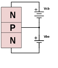
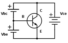
For a bipolar NPN transistor to conduct the Collector is always more positive with respect to both the Base and the Emitter. The voltage between the Base and Emitter ( VBE ), is positive at the Base and negative at the Emitter. The Base terminal is always positive with respect to the Emitter. Another way to display a NPN Transistor is shown in Figure 2 below.
The current flowing out of the transistor must be equal to the currents flowing into the transistor as the emitter current is given as
Ie = Ic + Ib. (1)
Note: “Ic” is the current flowing into the collector terminal, “Ib” is the current flowing into the base terminal and “Ie” is the current flowing out of the emitter terminal.
Since the physical construction of the transistor determines the electrical relationship between these three currents, (Ib), (Ic) and (Ie), any small change in the base current ( Ib ), will result in a much larger change in the collector current ( Ic ). The ratio of the collector current to the emitter current is called Alpha (α).
Alpha (α) = Ic/Ie (2)
The current gain of the transistor from the Collector terminal to the Emitter terminal, Ic/Ie, is a function of the electrons diffusing across the junction. The current gain of the transistor from the Collector terminal to the Base terminal is signified by Beta, ( β ).
Beta ( β ) = Ic/Ib (3)
NPN transistors are good amplifying devices when the Beta value is large. Beta values normally range between 20 and 200 for most general purpose transistors. Therefore if a transistor has a Beta value of 50, then for every 50 electrons flowing between the emitter-collector terminals one electron will flow from the base terminal.
By combining the expressions for both Alpha, α and Beta, β the current gain of the transistor can be given as:
Beta= (α)/(1-α) (4)
As seen from the equations above, electron mobility between the Collector and Emitter circuits is the only link between these two circuits. This link is the main feature of transistor action. Since transistor action is constituted by initial electron movement through the base region, the amplifying properties of the transistor comes from the consequent control the Base exerts on the current between the Collector and Emitter. As long as the flow of the biasing current into the base terminal is steady, the base region can be treated as a current control input.
PNP Bipolar Junction Transistor
A PNP Bipolar Junction Transistor has an N-doped semiconductor base in between a P-doped emitter and P-doped collector region. The PNP Transistor has very similar characteristics to the NPN Transistor, with the difference being the biasing of the current and voltage directions are reversed. For PNP Transistors, current enters into the transistor through the emitter terminal. A small current leaving the base is amplified in the collector output. The emitter-base region is forward biased so electric field and carriers will be generated. The voltage sources are connected to a PNP transistor are as shown in Figure 3 and Figure 4 below.
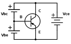
The voltage between the Base and Emitter ( VBE ), is now negative at the Base and positive at the Emitter. The Base terminal is always biased negative with respect to the Emitter while. The Emitter is positive with respect to the Collector ( VCE ). The reverse biased collector base part has generated holes. Due to the electric field, carriers or electrons get pulled by the holes. For a PNP transistor to conduct, the Emitter is always more positive with respect to both the Base and the Collector.
REGIONS OF OPERATION
Bipolar transistors have four distinct regions of operation. These regions are defined by the biases placed on the junction of the Bipolar Junction Transistor.
- Cutoff: The Cutoff region is when the transistor is inactive due to minimal current being passed through the transistor, which makes the transistor appear as an open circuit. Both VBE and VBC are reverse biased so all depletion region edges exhibit small minority carrier densities. This region has biasing conditions opposite of saturation.
- Forward-active: The Forward-active region occurs when the transistor is in its active state which allows the transistor to amplify the voltage variations present on the base. With the base-emitter junction is forward biased and the base-collector junction is reversed biased, the transistor can amplify voltage because the collector to emitter voltage is greater than the base to emitter voltage and is also in between the cutoff and saturation states. The output current is proportional to the base current and can be extracted at the collector.
- Reverse-active: The Reverse-active region occurs when the transistor is in its active state but the maximum current gain in the reverse active mode is much smaller than the forward active mode. The biasing conditions are reversed so that the base collector junction is forward biased and the base emitter junctions is reverse biased, which switches the roles of the collector and emitter regions. The base contains a much lower reverse bias voltage than in the forward-active region.
- Saturation: The saturation region allows the transistor to conduct current from the emitter to the collector. With both the base collector junction and the base emitter junction forward-biased, the base current is so strong it exceeds the magnitude at which it can increase the collector current flow. As a result, the circuit between the collector and emitter terminals appears to have short circuited due to the over saturation of current.
CONFIGURATIONS
There are three methods of connection for a Bipolar Junction Transistor within an electronic circuit. The Common Base configuration, Common Emitter configuration and Common Collector configuration all respond differently to the circuit’s input signal, thus varying the characteristics of each configuration.
The Common Base Configuration
The common base configuration has a strong high frequency response which is good for single stage amplifier circuits. However, is not very common due to its low current gain characteristics and low input impedance. The input signal gets applied between the base and emitter terminals while the output signal is taken from between the base and collector terminal. For this to occur, the base terminal has to be grounded so the reference voltage is a fixed amount. The Common Base Configuration is shown below.
This type of amplifier configuration is a non-inverting voltage amplifier circuit. The configuration has a resistance gain due to the ratio between the load resistance (Rload) in series with the collector and the Rin resistor. The input current flowing into the emitter is the sum of both the base current and collector current respectively therefore, the collector current output is less than the emitter current input resulting in a current gain. Its input characteristics represent that of a forward biased diode
The Common Emitter Configuration
The common emitter amplifier configuration produces the highest current and power gain of all the three bipolar transistor configurations which is why this type of configuration is the most commonly used circuit for transistor based amplifiers. The input signal applied between the base and emitter is small due to the forward biasing of the PN junction and the output taken from between the collector and emitter is large due to the reverse biased PN junction.
This is mainly because the input impedance is small as it is connected to a forward biased PN-junction, while the output impedance is large as it is taken from a reverse biased PN-junction. However, its voltage gain is much lower. The Common Emitter configuration is shown below.
The common emitter configuration is an inverting amplifier circuit. Therefore the output signal is out-of-phase with the input voltage signal.
The Common Collector Configuration
The common collector configuration is very useful for impedance matching applications because of the very large ratio of input impedance to output impedance. The configuration has the input signal directly connected to the base. With the emitter region in series with the load resistor, the current flowing through the load resistance is the same value as the emitter current. This is why the output is taken from the emitter load and the current gain of the configuration is approximately equal to the β value of the transistor.
This type of bipolar transistor configuration is a non-inverting circuit in that the signal voltages of Vin and Vout are “in-phase”. The load resistance receives both the base and collector currents which results in a large current gain as well as providing good current amplification with very little voltage gain.
Questions
1. If the collector current (Ic) is 50 Amps and the base current (Ib) is 2 Amps, then what is the Beta value?
2. What is the difference between a PNP Bipolar Transistor and a NPN Bipolar Transistor?
3. What is the current gain of the transistor is the given alpha (α) is 0.5?
Answers
1. The Beta ratio ( β ) = Ic/Ib. The Beta value is equal to 50 Amps divided by 2 Amps which is 25.
2. The PNP Transistor and NPN Transistor have very similar characteristics, with the difference between them being the biasing of the current and voltage directions.
3. The current gain of the transistor is the Beta ratio ( β ) which equals (α)/(1-α). The Beta value is equal to 0.5/(1-0.5) which equals 0.5
Additional Links
1. http://www.allaboutcircuits.com/textbook/semiconductors/chpt-4/bipolar-junction-transistors-bjt/
2. http://www.electrical4u.com/bipolar-junction-transistor-or-bjt-n-p-n-or-p-n-p-transistor/
References
1. Kasap, S. (2006). Principles of electronic materials and devices (3rd ed.). Boston: McGraw-Hill.
2. "NPN Transistor Tutorial - The Bipolar NPN Transistor." Basic Electronics Tutorials. 1 Sept. 2013. Web. 8 Dec. 2015.
3. "The Junction Transistor." The Junction Transistor. Web. 8 Dec. 2015.
4. All images were created using the software on digikey.com
Contributors
1. C. Beatty, MSE (University of California, Davis).